Low-power, high-performance active mixers for a variety of applications with low power consumption and 4GHz operating frequency allow WiMAX systems to convert frequencies from 3.3 to 3.8 GHz.
The LT5560 is a double balanced active mixer fabricated in a second generation high frequency bipolar process, resulting in high bandwidth and very low power consumption. All signal ports operate over a frequency range from almost DC up to 4 GHz, making it easy for upconversion and downconversion applications. In the case of proper matching, the upconversion conversion in the 2.5 to 2.7 GHz band and the upconversion to the 3.3 to 3.8 GHz WiMAX operating frequency can be realized at low cost, low power consumption, and high performance. Unlike most passive mixers with a conversion loss of a few dB and requiring a high LO drive level, this new active mixer not only provides conversion gain, but also requires only -2dBm of LO signal power. The core of the mixer can be operated from a single supply and is suitable for different voltages from 2.7 to 5.3V. The enable circuit provides fast and simple turn-on and turn-off operations to meet most TDD requirements. The LT5560's typical shutdown current is less than 1μA in a 3mm & TImes; 3mm 8-lead DFN package with grounded ground.
The IN, OUT, and LO ports are all differential ports for optimal performance. The IN and OUT ports must be used differentially, but the LO port can be driven with a single-ended signal and the unused LO pin is connected to ground through a capacitor.
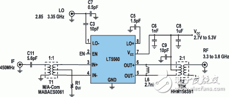
The LT5560 is suitable for both upconversion and downconversion. The circuit shown in Figure 1 is a practical upconversion application. The circuit has been fine-tuned for the 450MHz IF input frequency and the 3.3 to 3.8GHz RF output frequency. The LO port is fine-tuned at a frequency of 2.85 to 3.35 GHz.
At 450MHz, the differential impedance of the input ports (IN+, IN-) is approximately 28.6+j4.9Ω. The parasitic reactance caused by the board layout and T1 converts this impedance to approximately 50 Ω + j60 Ω. Capacitor C11 provides DC isolation and improves impedance matching by eliminating the imaginary part of the impedance. Transformer T1 has a 1:1 impedance ratio that provides single-ended to differential conversion of the input signal.
The mixer's signal input pin requires a DC path to ground, which is provided by resistor R1. In this application, a 0Ω resistor is used to allow the LT5560 to operate at maximum supply current to provide maximum gain and optimum OIP3 performance. Increasing the value of R1 reduces the supply current, but at the expense of reduced linearity and conversion gain.
At the RF output port, inductor L6 is used to eliminate the internal capacitance of the LT5560. The multi-layer chip balance converter T2 provides differential to single-ended conversion of the RF output signal. T2 also performs a 2:1 impedance transformation.
For convenience, the LT5560's LO input port can be driven with a single-ended signal. For upconversion applications, it is recommended to apply a signal to the LO-input (shown in Figure 1) to minimize the LO signal that leaks into the output.

Figure 1 Schematic diagram of 3.3 ~ 3.8GHz upconverting mixer application
The LO pin is biased by the internal reference and must be AC ​​coupled. Capacitor C3 provides the required DC isolation for LO-, while C7 is used to improve impedance matching. Capacitor C5 provides DC isolation on the LO+ pin and eliminates the parasitic inductance of the package by resonance to establish a good high frequency ground. This capacitor should be placed close to the LT5560 package for optimum performance.
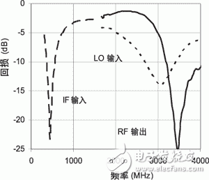
For this application, the return loss of the tested port is shown in Figure 2. The return loss of the IF port indicates that the impedance matching is good in the range of 375 to 550 MHz. The RF output port is well matched in the range of 3.25 to 4 GHz, and the return loss of the LO port is better than 10 dB in the range of 2.7 to 3.4 GHz.

Figure 2 IF, RF and LO port return loss
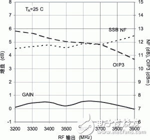
The test circuit is powered by a 3V supply and the measured DC current is 13.6mA. The input signal level of this circuit is -20dBm per frequency, and the applied LO power is? -2dBm. The conversion gain, OIP3 and SSB noise figure and LO input power change are shown in Figure 3.

Figure 3 Conversion gain, OIP3 and SSB noise figure and LO input power changes
In Figure 3, the conversion gain, OIP3, and SSB noise figure are a function of the RF output frequency. In this band, the conversion gain varies from approximately 0.2 to 0.6 dB, while the SSB noise figure varies from 11.5 to 12.1 dB. OIP3 is gradually reduced from 12.6dBm at 3.3GHz to 11.3dBm at 3.8GHz.

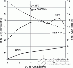
Figure 4 Conversion gain, OIP3 and SSB noise figure and LO input power change
In Figure 4, the conversion gain, OIP3, and SSB noise figure at 3.6 GHz are a function of the LO input power. The ideal range for LO input power is -4 to +1 dBm, but the noise figure is better at the higher end of this range. The gain (at TA = 25 ° C) is positive and gradually increases as the LO power increases as the LO power exceeds -4 dBm. The performance of the higher end of this ideal working range is determined by OIP3, and OIP3 begins to decline after exceeding +1dBm.
The measured results show that the LT5560 can form an excellent upconverting mixer in the frequency range of 3.3 to 3.8 GHz.
3.2v12-30Ah Lithium Battery Cells
3.2v12-30Ah Lithium Battery Cells,3.2v12-30Ah Lithium Battery Cells price,3.2v12-30Ah Lithium Battery Cells product
Jiangsu Zhitai New Energy Technology Co.,Ltd , https://www.jszhitaienergy.com
