Low-cost smartphones that are expected to continue to expand in the next two years are driving the development of the entire smartphone market. The widespread adoption of smartphones in emerging markets and the replacement of feature phones or basic handsets in mature markets are the development of this market. Driving factors. Subdivided low-cost smartphones enable multiple mobile handset manufacturers to enter the smartphone market by competing with Samsung, the number one mobile phone supplier in the high-end and low-end segments, The gap between them.
Equipment manufacturers competing in these markets must provide cost-effective smartphones and need to offer one or two satisfactory feature sets under their flagship smartphone products. For low-cost smartphone devices, such as waterproof devices or adding a heartbeat sensor and using high-performance storage are not required features. However, having high-quality front- and rear-facing cameras and a high-resolution display are key features—users expect to have them in their low-cost smartphones as well.
To provide low-cost, high-quality smartphones to new users in emerging and mature markets, manufacturers must have highly integrated hardware chips (ICs) that provide the high-end features they must have in a cost-effective manner. .
Therefore, smartphone device manufacturers must invest in system integration to reduce hardware costs. Lowering chip costs puts pressure on application processor vendors who are required to integrate as many of the system components as possible in their smartphones and to optimize the sub-segments of low-cost smartphones at a specific price range. System-on-a-chip (SoC).
While working to reduce costs and power consumption, designers must continue to push design innovation to a new world. Therefore, it is imperative to integrate the latest interface IP to optimize power consumption, cost and time to market.
Interface protocol for camera and displayThe Camera Serial Interface (CSI-2) and Display Serial Interface (DSI) protocols developed by the Mobile Industry Processor Interface (MIPI) Alliance based on MIPI D-PHY are widely used in mobile devices, which are low-cost smart The mobile segment offers a flexible, cost-effective solution; D-PHY connects image sensors and displays to SoCs in mobile handsets and embedded applications in MIPI CSI-2 and DSI applications Physical layer. They are the de facto standard interfaces between the application processor and the display (using the DSI protocol) or between the camera and the image sensor (using the CSI-2 protocol). The MIPI protocol is designed and optimized to meet the functional requirements of image sensors and display applications while minimizing cost and power consumption. D-PHY economically implements high-speed and low-speed data streams, which implements protocol layer connectivity through physical layer-protocol interface (PPI) connections.
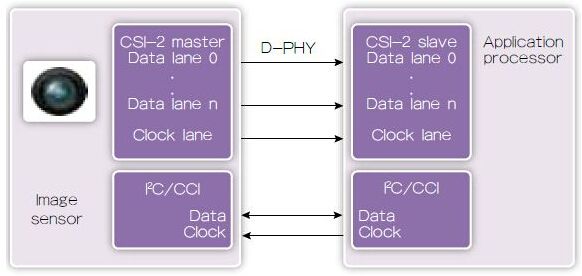
As shown in Figure 1, the CSI-2 is a high-performance serial interconnect bus for mobile applications that connects camera sensors to digital image modules such as host processors or image processors. The CSI-2 uses MIPID-PHY as the physical layer and high-speed differential interface, usually with several data channels (typically 1, 2, 4 or even 8) and a common differential clock channel. For configuration purposes, an I2C-based Sideband Camera Control Interface (CCI) is used to connect the signals between the control panel and the camera. The CSI-2 protocol supports the host and device interfaces required in application processors, camera sensors, and bridge applications.

Figure 1: MIPI Camera Serial Interface (CSI-2).

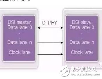
Figure 2: MIPI Display Serial Interface (DSI)
As shown in Figure 2, the DSI is a high-speed, high-resolution serial interconnect bus that provides connectivity to display devices. DSI uses the MIPI standard D-PHY as a physical layer high-speed differential interface with up to four data channels and one common differential clock channel. Pixel data and instructions are serialized into a separate physical stream, and the state can be read back from the display. The protocol supports the host and device interfaces required in application processors, display panels, and bridged applications. It also supports display devices running in video mode and command mode because the requirements in more complex and lower power implementations depend on system implementation and application. The command mode is required when the display controller and frame buffer are integrated on the display panel. The conversion usually takes place in the form of an instruction followed by a data pixel/parameter. In command mode, the host can write and read out panel registers and frame buffers, and when converted in video mode, pixel data is transferred from the host to the panel in real time.
Drive higher data ratesMost of the image and display sensors available on the market today have been developed over the past five to seven years, supporting high-speed burst modes of up to 1,000 Mbps per channel. Several devices are in volume production and support speeds in excess of 1,000 Mbps because the goal is to increase bandwidth on the same number of connection contacts.
The recently released MIPI Alliance D-PHYv1.2 specification extends the high-speed burst capability of D-PHY to 2.5Gbps per channel. Developers of display and image sensors can now take advantage of the same design and architecture to support aggregated bandwidths of up to 10 Gbps using four data channels, or use eight data channels with minimal modifications to support 20 Gbps data rates. The use of long-standing, proven, multi-vendor-developed and constantly evolving architectures provides a fast, low-risk way to achieve the desired bandwidth, time-to-market, and low-cost goals.
Drive lower power consumptionThe scalability of D-PHY helps save power. It uses many optional data channels and closes unused data channels. In most cases, the data channel operates in unidirectional mode for high-speed transmission. At this time, a Mas terD-PHY and a Slave D-PHY source and receive clocks, respectively. For example, a DSI host application implemented on the SoC side uses a MasterD-PHY to send signals to the display as a source on the board, while a CSI-2 host application uses a Slave D-PHY to receive signals from the image sensor.
Because the D-PHY is not tied to a particular rate, it can optimize power consumption based on the generated traffic when looking for a clock signal that is related to the actual required data rate. This flexibility creates a cost-effective solution by eliminating the need for unnecessary memory caching and design complexity. In addition, DPHY supports high and low speed (or low power) operation. High-speed transmission uses a clock channel, while low-power operation mode uses its own clock data to conserve power while the clock channel remains idle.
Drive lower costsThe MIPID-PHY v1.2 specification includes enhancements to provide various throughputs for higher bandwidth image and display sensors, but it also helps reduce costs.
The ability to send the same amount of data with fewer data channels helps reduce chip area and use fewer pins, all of which are directly related to the chip cost of the application processor. The application processor needs to be connected to an image sensor at 4 Gbps, and can use two data channels running at 2.0 Gbps instead of four data channels running at 1.0 Gbps. When this method of reducing the number of channels and pins is used for several image sensors, the cost of the chip and package will be significantly reduced.
to sum upSynopsys' DesignWare MIPI IP has enabled many SoC developers to achieve volume production through the use of D-PHY, CSI-2 and DSIIP. Design Ware MIPID-PHYv1.2 IP significantly reduces area, cost and power consumption. The IP minimizes time-to-market and maximizes ROI for CSI-2 and DSI applications with configurability options and rich solutions, while reducing the SoC design required to support multiple applications Quantity.
The monitor is a part of the closed-circuit monitoring system (CCTV). It is the display part of the monitoring system and the standard output of the monitoring system. With the display of the monitor, we can watch the images sent from the front end. As an indispensable terminal equipment of video surveillance, it ACTS as the "eye" of surveillance personnel and plays a key role in the post-inspection.
The traditional CRT monitor has advantages over the existing LCD in brightness, contrast and visual Angle, etc., but with the technical progress of LCD, its brightness and contrast have been improved to the level comparable to THE CRT, while the Angle of view of the existing LCD screen has been close to the absolute Angle of view, and there is no gap with the CRT. LCD monitors have advantages over CRT monitors in light weight, environmental protection and low energy consumption. In addition, LCD monitors can eliminate many problems of CRT monitors, mainly in five aspects:
1.LCD monitor can completely eliminate the problem of burn, that is, the long-term static and highlighted picture attenuates the fluorescence of CRT monitor, thus generating the phenomenon of ghosting.
2. The LCD monitor will not flash at all.
3. No aggregation of LCD monitor.
4. The LCD monitor is not magnetized and does not need to be eliminated.
5. The LCD monitor adopts fixed pixels, which will not produce geometric distortion.
Elo Open Frame Monitor,Open Frame Capacitive Monitor,10 Inch Open Frame Monitor,Lcd Monitor Open Frame
TONYA DISPLAY LIMITED , https://www.tydisplay.com
