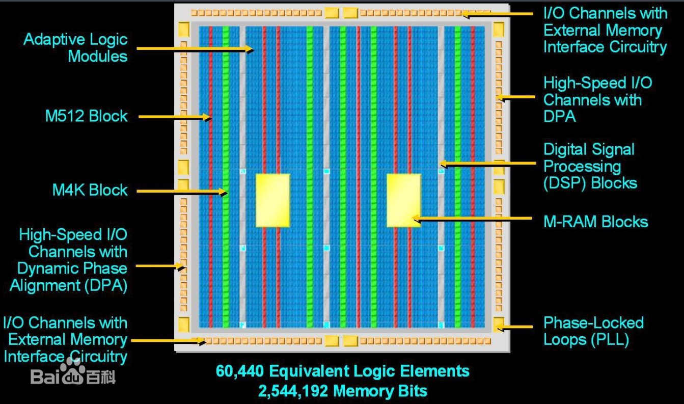
Learn the simple design method, learn module design and module division techniques.
Module division, as the name implies, refers to the division of modules. However, the module division proposed by Ming Deyang to the simplified design method is a broad "module division." The "module division" mentioned later refers not only to the division of the module, but also to the determination of the data flow direction between the module's ports and modules after the modules are well-divided.

Module division principle
Principle 1: Registers are used for the output of the sub-modules of each synchronous timing design.
Principle 2: Divide related logic or reusable logic in the same module.
Principle 3: Separate the logic of different optimization goals.
Principle 4: The logic of loose constraints is assigned to the same module.
Principle 5: Separate the storage logic into modules.
Principle 6: The appropriate module size.
The module partitioning technique is very important. A good module structure can greatly simplify the structure of each module, so that the required functions can be realized with the least code; the modules can run smoothly and the system can be more stable. We all know that ISO and Android are the most important features. Although any mobile phone function can be implemented on both systems, the stability and efficiency of ISO far exceed that of Android. This can be attributed to ISO's good system architecture. It can be said that the module division further explores the wisdom of the people. The Chinese have not designed a good chip structure so far. Huawei's architects are basically foreign experts.
How to divide the module, listed a lot of practical skills.
1. Describe the common signals for the connection between modules. General module connects through these signals, the reader basically defines these signals when defining the module signal, and do not need to worry about the naming problem of the signal.
2. For FPGA internal modules, several modes and application scenarios for data interaction between modules are described. Readers can choose the appropriate mode to use according to the project situation.
3. The FPGA often communicates with peripherals. The simplified design method also describes the FPGA module standard when it is connected to a peripheral device. Generally, it can be divided into an interface module and a command module. The interface module is responsible for timing, and the command module is responsible for issuing commands.
4. For complex, internally-registered peripherals. The simple design defines the module standard, which is convenient for debugging and use, but also reduces the possibility of error.
The simplified design method that has been studied has comprehensively considered the debugging, use, and error-rejection rates, so that each student can design the best code.
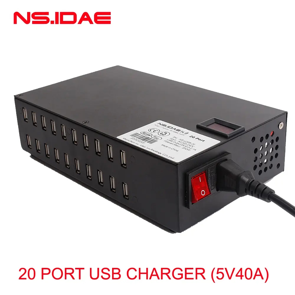
20 port USB charging station
This 20 port USB charging station has high quality patience and persistence. And the maximum demand that meets the charging is up to 20 devices. Each interface has an independent chip, which effectively prevents mutual interference between each port. Static single fan automatically heat dissipation to ensure the safety of the charging equipment. Provide overvoltage, short -circuit, overload, overload, temperature and voltage regulator protection.

20 Port Usb Charger,Usb Ai Smart Charger,20 Port Intelligent Charger,20 Port Electronic Devices Charge
shenzhen ns-idae technology co.,ltd , https://www.szbestchargers.com
