introduction
For new digital systems, backing up important data during a power outage is an important feature. Data loss is a concern in telecommunications, industrial and automotive applications where embedded systems rely on clean uninterruptible power supplies. A sudden interruption in power supply can result in data corruption while the hard drive and flash memory are being read or written. Data storage is widely used in embedded systems for automotive maintenance, troubleshooting and repair work. In complex industrial metalworking equipment, it is extremely important to store the location and state of the various tools after the power is disconnected to prevent equipment failure when power is restored.
Traditionally, backup power designers have relied on the presence of high-voltage power supplies and large-capacity capacitors in boost-type power factor correction (PFC) circuits. When using this conventional approach, the available energy in the combination of the 350V to 400V PFC output voltage and the very large capacity capacitor during the power interruption is sufficient for the downstream converter to support the critical load for the required hold time. Keeping time is simply the time it takes for the system to safely complete the backup operation.
The problem is that many new electronic systems (eg cars) do not require an AC/DC converter. In addition, the nature of PFC has changed dramatically: in low-power and distributed systems, small-area isolated flyback converters are gradually replacing the “boost-boost†converter pair. In these environments, low voltage power supplies are often the only available power source for backup devices.
All batteryless backup solutions are based on the ability of capacitors to store energy (W).


C is the capacitance; V MAX and V MIN are the maximum and minimum capacitor voltages; V OUT and I OUT are the load voltage and current; T H is the hold time, that is, the power supply can keep the output voltage regulated after the power supply is interrupted. The time of the state.
Three simple power supply retention solutions
To meet hold time requirements in low voltage systems, designers can add capacitance (often by using supercapacitors) or use a boost converter circuit to generate a higher voltage. Both solutions are very easy to implement with a conversion IC designed to support them, but they require additional components in addition to the standard DC/DC conversion circuitry. This article describes two representative circuits of the above solution, and a "cheaper" solution for relatively short hold times (the solution does not require the use of additional controllers or capacitors).
Supercapacitor-based power retention solution
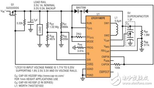
Let's look at an easy-to-implement supercapacitor solution based on the LTC3110 2A bidirectional buck-boost DC/DC regulator and charger/balancer (see [1] for details). The electrical principle of this solution is shown in Figure 1.

Figure 1: Ultracapacitor-based LTC3110 backup solution ( VIN up to 5.25V)
In Figure 1, the load and buck-boost LTC3110 converters are powered by the input voltage of MOSFET Q1, which is normally on. When V IN is connected, the LTC3110 charges and charges the supercapacitor. In this circuit, a three terminal supercapacitor is a combination of two stacked capacitors. During charging, the LTC3110 safely balances the supercapacitors to equalize the voltage across each half of the stack to avoid overvoltage conditions.
When V IN is interrupted, Q1 is turned off, thereby isolating the load from the original voltage supply, and the LTC3110 releases the stored energy of the supercapacitor to the load. In this case, the LTC3110 maintains a stable 3.3V rail voltage, even when the supercapacitor voltage drops from its full 5V value to well below 3.3V (see [1]). Resistors R DT , R DB are responsible for controlling the direction of energy flowing to or from the storage capacitor, R FT , R FB set the load voltage, and R BT , R BB set the maximum voltage across the storage capacitor. Despite the use of supercapacitors, this solution can support flat applications up to 1mm high, see Figure 1.
Boost voltage retention solution
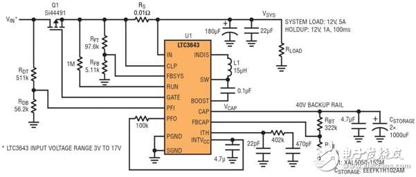
Figure 2 shows an example of a solution that uses a much cheaper (compared to a supercapacitor) electrolytic or hybrid storage capacitor, but with a much higher voltage across them. This backup solution is centered around the LTC3643 (see [2]). The regulator boosts the input voltage to 40V (max) when the input is present. When an input is interrupted, the LTC3643 operates as a buck regulator that discharges the storage capacitor's power to the load but maintains the programmed voltage level. The resistor divider described in the above supercapacitor solution has the same function here.

Figure 2: LTC3643 high voltage backup solution; VIN up to 17V
The above supercapacitor solution and this higher voltage solution both reduce the capacitor charging current and are designed to keep the input current below or at some preprogrammed value and set the load demand to a higher priority than the storage. Capacitor charging time. This is especially important in systems with relatively high input impedances (eg battery powered systems) or systems powered by low power AC/DC or DC/DC converters. In the LTC3110 supercapacitor solution, this function is implemented by the resistor R PR ; in the higher voltage LTC3643 solution, it is implemented using the current sense resistor R S .
"cheaper" power retention solution with a minimum number of components
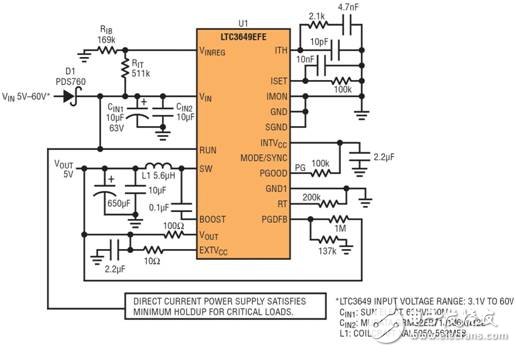
For projects that require relatively short hold times and are cost sensitive, the solution in Figure 3 replaces the minimum component cost by reducing hold time. This solution is centered around the LTC3649, which acts as a buck converter in general. But here, the LTC3649 goes to perform a boost conversion operation when the input voltage is disconnected. The LTC3649 maintains the programming voltage on the critical load terminals by discharging its own output capacitor.

Figure 3: LTC3649 "cheaper" backup solution with VIN up to 60V
in conclusion
The solution presented in this paper focuses on DC/DC power supply retention systems covering a wide input voltage range: 1.8V to 5.5V (using LTC3110), 3V to 17V (using LTC3643), and 3.1V to 60V (using LTC3649). All three solutions can be successfully used in automotive and industrial applications where data backup is required in the face of input power interruptions.
references
1. http://LTC3110,
LTC3110 Product Manual and Demo Circuit.
2. http://LTC3643,
LTC3643 Product Manual and Demo Circuit.
3. http://LTC3649,
LTC3649 product brochure and demo circuit.
RJ45 JACK+USB Section,60 Jack.Professional RJ45 Connection Guide manufacturer is located in China, including RJ45 Connection Order,RJ45 Wall Jack Installation,RJ45 Modular Jack Wiring, etc.
1 , with or without transformers
2 , with or withour PoE function
3 , Customized length of Pin
4 , Customized housing color
5 , Customized contact area gold plating
6 , Customized LED Indicator color
The RJ-45 interface can be used to connect the RJ-45 connector. It is suitable for the network constructed by twisted pair. This port is the most common port, which is generally provided by Ethernet hub. The number of hubs we usually talk about is the number of RJ-45 ports. The RJ-45 port of the hub can be directly connected to terminal devices such as computers and network printers, and can also be connected with other hub equipment and routers such as switches and hubs.
RJ45 JACK+USB
ShenZhen Antenk Electronics Co,Ltd , https://www.antenkconn.com
