Distributed amplifiers provide a wide frequency range and high gain. For some time, its design typically used transmission lines as input and output matching circuits. Bill Packard (one of the founders of Hewlett-Packard) proposed a vacuum tube amplifier circuit based on distributed design in his paper in 1948. With the development of gallium arsenide (GaAs) microwave monolithic integrated circuits, in order to improve efficiency, output power, and noise figure, many types of amplifier circuits have been proposed, but distributed amplifiers are still broadband circuits (such as optical communication). The mainstream design of the circuit). Understanding the design of GaAs MMIC distributed amplifiers for GaAs microwave monolithic integrated circuits will be of great help to many broadband circuits.
Johns Hopkins University from 198? Since the beginning of the year, the MMIC design course has been opened and students are allowed to stream on TriQuint's production line. A distributed amplifier designed by Craig Moore (who served as a teaching assistant for the course from 198 to 2003) is a classic design example of the course. The design even went through low temperature environmental experiments and exhibited a lower noise figure at low temperatures in liquid nitrogen. The amplifier uses TriQuint's 0.5μm GaAs MESFET process, which has a slightly lower gain than the new circuit based on the 0.5μm GaAs pseudo-high electron mobility transistor PHEMT. In the new course in 2006, a new version of the 0.5μm GaAs PHEMT distribution amplifier was used. And some other circuits as an example. This article will introduce the design method of the wideband amplifier and the results of simulation and measurement.

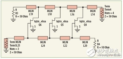
Figure 1: Schematic diagram of a distributed amplifier circuit using a microstrip transmission line.
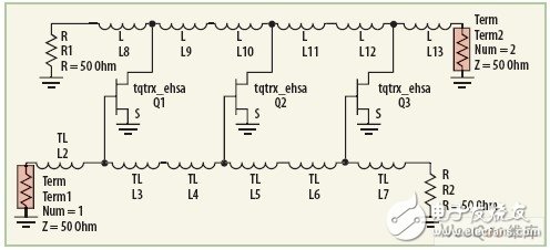
A distributed amplifier uses a broadband transmission line to inject an input signal into a set of active devices (see Figure 1), while another parallel transmission line collects the output signals of each active device and superimposes them. Each stage provides a comparable gain, but the gain is distributed over a wide frequency range. Compared to a cascaded design, the total gain is the sum of the gains at each stage, not the product of the gains at each stage. However, when lumped parameter components are used to approximate the distributed transmission line (see Figure 2), the lumped parameter transmission line's shunt capacitance to ground is replaced by the parasitic capacitance of the transistor. The equivalent transmission line of the lumped parameter component is used as a low-pass filter whose cutoff frequency is inversely proportional to the parasitic capacitance of the transistor. Therefore, the size of the transistor directly determines the upper limit of the operating frequency of the circuit. The various parameters that the design always considers together include: the number of stages of the amplifier, the size of the active device, the type of process of the device (if there are multiple types), and the DC offset for each stage. More series means a larger gain-bandwidth product, but it also introduces more power. Once the size of the transistor is determined, simulation software can be used to optimize parameters such as gain, reflection coefficient, output power, and noise figure.

Figure 2: Schematic diagram of a distributed amplifier circuit using lumped parameter components (where CGS and CDS represent gate capacitance and drain capacitance, respectively).
Due to the many applications of distributed amplifiers, the requirements for various performance indicators are very flexible, and broadband gain is one of the most important indicators. In the Craig Moore design example, an enhanced PHEMT device was used because the enhanced device only requires a set of positive voltage supplies. In order to be able to provide and 198? The same performance of the circuit used by TriQuint Semiconductor in the 0.5μm GaAs MESFET process, which uses a 0.5μm GaAs PHEMT process and uses a 3-stage transistor to amplify the topology. In order to adapt to battery-powered applications, 3.3V is used. Of course, in order to meet different customer needs, the operating voltage and current can be conveniently adjusted over a wide range. At 1.5V and 14mA, the simulation results show that only 2dB of gain is lost, and the gate voltage is 1.5V to 5.0V, and the change in performance is small when the drain current varies between 14~35mA. For optimal gain and matching performance, use Agilent? The computer-aided engineering software ADS performs linear simulation to determine the appropriate inductance value and PHEMT size.

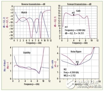
Figure 3: Simulation results of the matching, gain, noise figure, and stability factor of the PHEMT distributed amplifier.
Through the ideal simulation calculation, the design uses 6&TImes; 30μm enhanced PHEMT device, Craig Moore's 198? In the design of the year, some additional matching components were added to the drain of the MESFET tube to ensure that the effective output capacitance and the gate input capacitance were the same. At this point, the lumped parameter transmission lines of the input and output will be symmetrical and have the same phase delay. The article also compares this input and output transmission line symmetrical matching scheme with another leakage capacitor independent optimization scheme (drain inductance and gate asymmetry). For this simple 3-stage PHEMT design, the phase shift difference between the gate and drain input lines is small, and a simpler asymmetric scheme is used here. If the phase difference between the input and output transmission lines is large, this scheme cannot effectively combine the gains of the stages. Next, use TriQuint's inductors, resistors, capacitors, and interconnect models to replace the ideal components for more realistic simulation. Figure 3 shows the gain, matching, stability factor and noise figure of the desired final amplification circuit. The simulation uses a 30mA and 3.3V DC bias design to limit its power consumption to within 100mW and achieve a compromise between output power and third-order intermodulation cut-off point. Figure 4 shows the layout of the circuit. It also includes two test model tubes with probe access: one for the 6&TImes used in the design; the 30 μm enhanced PHEMT for the design, the other for the common 6 & TImes; and the 50 μm depletion PHEMT.
Butt Connector,Lugs Insulated Female Connectors,Insulated Female Connectors,Non-Insulated Spade Terminals Wire Connector
Taixing Longyi Terminals Co.,Ltd. , https://www.longyiterminals.com
