The operational amplifier is one of the most widely used components in the design of electronic circuits. Although simple in function, they exhibit complex behavior because the op amp itself is an elaborate subcircuit made up of a dozen transistors. The ideal op amp models, namely infinite gain, bandwidth, input impedance and output admittance, and zero-valued input offset voltage and bias current, are good first-order approximations of Op Amp-based circuits. .
According to the operational environment of the op amp, it can analyze its deviation from the ideal behavior. The DC measurement system is such an environment. In this application, the existence of offset voltage can not be ignored. Unlike a signal processing chain, a capacitor can easily be used to filter out DC offsets in the signal processing chain. The offset voltage of the op amp can cause output errors of the dc signal. In addition, if the offset voltage values ​​are not negligible, they can reduce the dynamic range of the output. Various documents and textbooks describe the existence of offset voltages.
This paper presents a general method for calculating the output offset when the op amp used in the circuit has an input offset amount e.
The transfer function of an ideal op amp is described by the equation y = A(V+ - V-), where y is the output, A is the gain, and A→∞, and V+ and V- are the voltages at the positive and negative input terminals of the op amp, respectively. Assuming that the actual op amp input/output transfer characteristic is y = A(V+ - V- + e), where e is the differential input error of the ideal op amp, the amount of misadjustment can be calculated.
This model is consistent with the results observed in real op amps: when the input is different (V+ ≠V-), the output is zero; when V+ = V-, the actual op amp produces a non-zero output. Assume that the function model of the op amp is y = A(V+ - V- + e), where e is the input offset voltage. When used in a negative feedback configuration, we get:

Or, for any op amp used in a negative feedback configuration, V+ - V- = - e (assuming infinite gain).
Therefore, the "golden rule" of op amps widely followed when analyzing ideal op amp circuits needs to be modified to include a value e that indicates the presence of an input offset voltage.
• In a circuit that uses negative feedback to configure the op amp, V- = V+ + e; • The op amp positive or negative input/output current is zero.
Now consider the circuit topology shown in Figure 1. The schematic topology maps to the circuit shown in Figure 2. The resistance network is replaced by the Thevenin equivalent circuit (looking from the terminals) with Vth+, Rth+, and Vth-, Rth-.
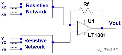
Figure 1: General topology of a negative feedback op amp circuit.
Apply the golden rule:
V− = V+ + e = Vth+ + e because V+ = Vth+. Applying Kirchhoff's current law to the negative terminal of the op amp in Figure 2 yields:

Solve Vout with Vth+, Vth-, and e to get:

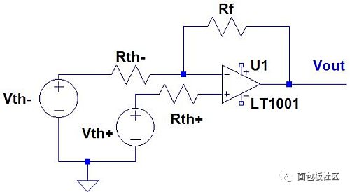
Figure 2: The circuit topology shown in Figure 1 is mapped to this circuit.
F(Vth+, Vth-, 0) is just the output of the ideal op amp (ie, the input offset voltage is zero). Therefore, the output offset is:

We will apply the above derived formula to the output offset calculations of various op amp circuits that are widely used.
Differential amplifier
See Figure 3. under these circumstances:
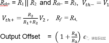
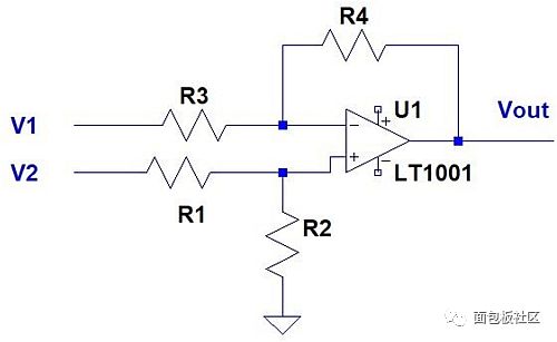
Figure 3: Differential Amplifier.
1a. A special case of a non-inverting amplifier differential amplifier with V1 = 0 and R1 = 0.
Summing amplifier
See Figure 4.
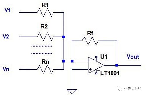
Figure 4: Summing amplifier.
In this case, Rth- = R1 || R2 || R3 ..........|| Rn, so:
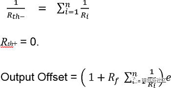
2a. Special case of sum amplifier in inverting amplifier, n = 1.
2b. Special examples of summing amplifiers shown above in binary-weighted DACs, where:

3. R-2R ladder digital-to-analog converter
As we all know, the equivalent output resistance of the R-2R trapezoid is R, independent of the length of the trapezoid. Figures 5 and 6 show two implementations. In Figure 5:

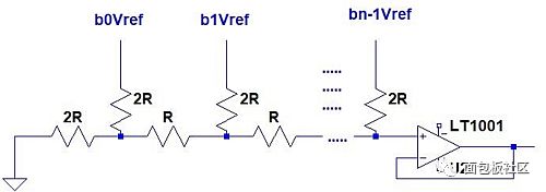
Figure 5: R-2R ladder digital-to-analog converter with buffered output.
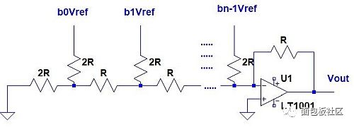
Figure 6: R-2R ladder digital-to-analog converter with inverting output.
In Figure 6:

When the value of n is small, the weighted binary DAC produces a smaller output offset than the R-2R DAC in FIG. 6 .
Consider bias current
The offset calculation in this section takes into account the bias current. Assume that the bias currents flowing out of the positive and negative terminals are IB+ and IB- (+ is the output current), respectively. Refer to Figure 2.

Applying Kirchhoff's current law at the negative end of the op amp yields:

Solve Vout with Vth+, Vth-, e, IB+, IB-, and get:

F(Vth+, Vth-, 0, 0, 0) is the output of the ideal op amp. Therefore, the output offset is given by:

After calculating Rth+ and Rth- for each of the above cases, the calculation of the total misalignment is simply to substitute the appropriate value into the above equation.
45W Pd Charger,Pd 45W Fast Charger,45W Pd Wall Charger,Plug Pd 45W Fast Charger
Guangdong Mingxin Power Technologies Co.,Ltd. , https://www.mxpowersupply.com
