At present, the medium and small-scale LED display systems on the market generally use the traditional single-chip microcomputer as the main control chip. For LED large-screen displays, due to the large amount of data transmission, the scanning speed is required to be fast, while the internal resources of the microcontroller are low and the operation speed is slow, and it is difficult to meet the system requirements. FPGA is used as a controller. On the one hand, FPGA uses software programming to realize hardware functions, and it is faster. On the other hand, it has rich pin resources and strong scalability. Therefore, the use of a single FPGA and a simple peripheral circuit can achieve large-screen LED display control, without the need to design a separate Chinese character library, with high integration, stability, design flexibility and high efficiency.
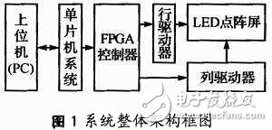
1 Overall structure of the systemLED large-screen display system consists of upper computer (PC machine), single-chip microcomputer system, FPGA controller, LED display screen rank driving circuit and other modules, as shown in Figure 1. The host computer is responsible for the collection and transmission of data such as Chinese characters and characters. The asynchronous serial communication between the single-chip microcomputer system and the host computer works through the serial port to obtain the graphics dot matrix data to be displayed which has been completed format conversion from the host computer, and stores it in the EEPROM memory. Afterwards, through the FPGA controller, the display data of the memory is restored to the LED display screen. The scanning control circuit adopts the programmable logic chip Cyclone EP1C6, uses the VHDL language programming to realize, adopts 1/16 scanning mode, the refresh frequency is above 60 Hz. This article focuses on the 256 & TImes; 1024 monochrome graphic display FPGA control module.
For large-screen LED displays, the column display data is usually used in the serial transmission mode, using 1/16 scanning. Figure 2 shows the basic structure of the 16&Times; 32-bit array cell module. The column drive circuit is made up of four 74HC595 cascades. Under the action of the shift pulse SRCLK, the serial data is input one bit at a time from the data port SER of the 74HC595. When all 32 columns of data in one row are transmitted, the latch signal RCLK is outputted and the pass signal Y0 is selected. Rows of data can be displayed as required. The remaining lines are displayed in the same way. After 16 lines of data are scanned once (ie, one cycle is completed), the next cycle is scanned from the first line. The display does not flash as long as the scan period is less than 20 ms.
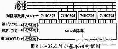
256 & TImes; 1024 large-screen display by 16 & TImes; 32 16 × 32 dot-matrix screen cascade. In order to shorten the signal transmission time from the control system to the screen body, the display data is divided into 16 zones, each zone is composed of 16×1024 dot matrix, each line of data is 1024/8=128 bytes, and the pixel signal of the display screen consists of The right side of the LED display shifts to the left, leaving the 16 partitions of data in the same memory. The display data of one screen is 32 KB. To accurately read the data of 16 partitions, the read address of the memory is composed of 16 bits. Since the data is only 32 KB, the highest value can be set to 0. The remaining 15 bits from highest to lowest are: row address (4 bits), column address (7 bits), and partition address (4 bits). The decode signal (Y0 to Y15) of the 4-bit partition address functions as a latch pulse of the latch, and sequentially latches the first byte data of the 1st to 16th partitions to the corresponding lock in the 16 read address generation cycles. The register then latches the 16 bytes of data at the same time into 16 8-bits and shifts into the shift register bank at the rising edge of the shift latch signal. A clock cycle occurs at the next 16 read addresses. On the one hand, the serial shift register is used to shift the 8-bit data to a serial output. The shift clock is the read-address-occurring clock divided by two. On the other hand, 16 clocks are used in sequence. The second byte data of the partition is read out and latched into the corresponding latch, and after all the first row data of all the partitions are sequentially read out according to this rule, all serial shifts are performed at the rising edge of the data valid pulse signal. Data output, drive LED display. Next, the data in the second row is shifted and the first row remains displayed during this period; after the second row is all moved in, the second row is displayed, and the third row is moved at the same time. Complete the scan display of the entire LED large screen.
 3 FPGA-based display controller design
 3.1 FPGA control module overall plan
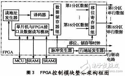
As shown in Figure 3, the FPGA control module is mainly composed of a microcontroller and an FPGA interface and a data read/write module, a read address generator, a decoder, a row address generator, a data latch group, a shift register group, a pulse generator, etc. Module composition.
The read address generator mainly generates the read address signal, and the address signal is sent to the MCU interface and the data read/write module, reads the processed LED display data in the external SRAM1 or SRAM2, and sends the data to the data latch according to the partition mode. Group latches. Latch output 16 partition data, through the shift register group to achieve parallel serial conversion to obtain the serial data required by the display, and sent to the LED display column drive circuit. The pulse generator provides corresponding synchronous clocks for each module, and the row address generator generates corresponding row signals to the row driving circuit of the display screen.
3.2 microcontroller and FPGA interface and data read and write modules
MCU and FPGA interface and data read and write module structure shown in Figure 4. After the microcontroller reads data from the EEPROM and processes it according to the display requirements, it sends the data to the data buffer SRAM1 or SRAM2 through the interface and the data read/write module. In order to improve the data transmission speed and ensure the continuity of the display effect, the dual-body switching technology is used in the system to complete the data storage process. That is, using a dual SRAM memory structure, two completely independent read and write address lines and data lines are switched in and out. During operation, the FPGA reads the displayed data from only one of the two SRAMs at a specific time for display, while another SRAM performs data exchange with the MCU. The MCU will write new data and work alternately in turn to achieve left, up, and dual display modes. If the displayed content does not change, that is, if the data in one SRAM does not change, the MCU does not need to write data to another SRAM.
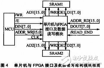
The module is implemented using a VHDL finite state machine. The entire control is divided into four states. The state transition diagram is shown in Figure 5. Its working process is as follows: System boot enters the initial state ST0, the write enable end of the one-chip computer is low, the one-chip computer reads the data from EEPROM and writes the data to SRAM1, at the same time FPGA reads the data in SRAM2; After the one-chip computer data finishes writing a screen data, E changes to high level, when FPGA finishes reading data from SRAM2, the end signal READ_END is low level, enter ST1 state.
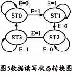
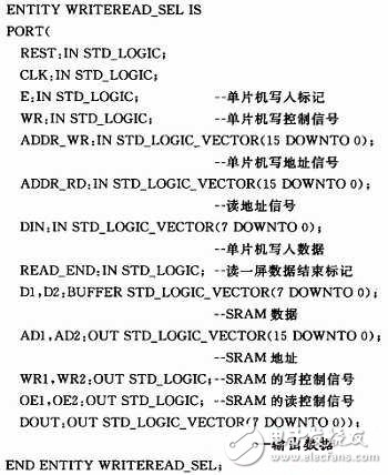
In the ST1 state, if no new data is written, E remains high, and the FPGA reads data from SRAM1 for static display; only when the read control signal E of the microcontroller is low and READ_END is low level. Enter ST2 state. Under ST2 state, the one-chip computer writes the data into SRAM2, FPGA reads the data of SRAM1 at the same time, after the one-chip computer data finishes writing, E turns into high level, when FPGA one screen data reads, READ_END is low, enter ST3 state. In the ST3 state, if no new data is written to E high, the FPGA reads the data in SRAM2. When the microcontroller has new data to write, E goes low, and when READ_END is low after reading one FPGA data, it will re-enter the ST0 state. Through this alternating cycle of writing and reading data, its port program is as follows:
3.3 Read address generator
The read address generator mainly generates a read address signal of the external buffer SRAM1 (SRAM2) so that the system can correctly read the corresponding display data from the memory. The most significant bit of the address is 0, and the remaining addresses are the row address (hang[3..0]), the column address (lie[6..0]), and the partition address (qu[3..0]) 15 effective addresses. signal. The 16-byte data in SRAM1 (SRAM2) is read out in 16 pulse cycles, and part of the VHDL source program is as follows:

3.4 Decoder
The decoder module is mainly used to generate 16 channels of partition signals (active low) to control 16 latches, respectively, and latch the display data of 16 partitions in corresponding latches.
3.5 Data Latch Group and Shift Register Group Module
The data latch group module consists of 16 8-bit latches that form a latch group that latches 16 partitions of data. The shift register block consists of 16 8-bit shift registers. It converts 8-bit parallel data in each latch into 16 serial data output at the same time, drives the LED display screen, and realizes data parallel-to-serial conversion.
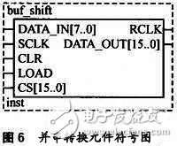
The resulting component symbol is shown in Figure 6. Among them, DATA IN[7. . 0] 8-bit parallel data input for each partition, SCLK is the shift clock, CLR is the clear signal, LOAD is the data latch signal, CS[15. . 0] is a 16-zone input signal (connected to the decoder output), DATA_OUT[15. . 0] 16-channel serial data output.
3.6 Pulse Generator
The system adopts the 1/16 scanning method, divides the data into 16 districts, 16 sections of data are conveyed at the same time. Assuming a refresh rate of 60 Hz (that is, a period of 16.67 ms), each line displays a time of approximately 16.67 ms/16 = 1.04 ms. With 1024 bits per line, the shift pulse period is 1.04/1024 = 1.02 μs, which means that the shift frequency is 0.983 MHz or more to meet the requirement. Since the shift pulse is a 2 frequency division of the data read module clock, the system clock is at least 1.97 MHz. This system uses a 50 MHz clock source. The timing diagram is shown in Figure 7.
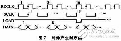
Among them, RDCLK reads the data clock for FPGA; SCLK is the shift clock of the serial output, it is 2 frequency divisions of RDCLK; LOAD is the data to latch the signal, after reading the data DATA of each byte in 16 districts after each reading A latch signal is generated and the data is latched in the data latch group. The clock is divided by 16 by RDCLK.
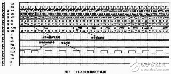
4 FPGA control module simulation testCreate a project in the QuartusII 5.1, and create a schematic file, interface with the microcontroller and FPGA and data read and write modules, read address generator, decoder, row address generator, data latches, shift registers, The symbols of the module elements generated by the unit modules such as the pulse generator are connected together to form the logic diagram of the total control module and the function simulation thereof. The simulation result is shown in FIG. 8 , 16 bytes of data are read from the memory, and 16 channels of serial data are output by parallel-serial conversion. From the waveform analysis, the function is correct, and each output port signal meets the timing requirements.
FPGA is an online programmable chip that can be programmed differently according to different user requirements, shortening the development cycle of the system and saving the development cost of the hardware. In this paper, FPGA is the main chip, and a large-screen LED monochrome graphic display control system is designed. With the development of LED display technology, the combination of FPGA and ARM or DSP chip will be widely used in the field of two-color display and color display.
NINGBO LOUD&CLEAR ELECTRONICS CO.,LIMITED , https://www.loudclearaudio.com
