The AD9854 integrates a 48-bit frequency accumulator, a 48-bit phase accumulator, a sine/cosine waveform table, two 12-bit high-performance quadrature D/A converters, and a modulation and control circuit that can complete the frequency on a single chip. , phase, amplitude modulation, and l|Q quadrature modulation. Driven by the high stability clock, the AD9854 will generate high-frequency, phase, and amplitude stable sine and cosine signals through digital programming as the local oscillator for communications, radar and other aspects. The AD9854 DDS core has a 48-bit frequency resolution (with a resolution of up to 1uHZ at 300M system clock). Outputting a 17-bit phase cutoff guarantees a good spurious-free dynamic range specification. At the same time, AD9854 also contains a programmable clock multiplier, which allows the lower-frequency oscillator to achieve an integer multiplier from 4 to 20 to the system clock signal through a multiplication circuit, with an internal clock rate of up to 300 MHz. When the system clock is 300MHz, the frequency resolution of the output signal can still reach 0.001Hz. Its circuit structure makes its maximum output frequency of 150MHz, and the output frequency adjustment rate reaches 100M times per second. The output sine wave signal can also pass the phase resolution of the on-chip high speed ratio bit, that is, the highest phase resolution is 360*/214. In terms of signal amplitude control, the AD9854 features a 12-bit digital multiplier that provides 12-bit output amplitude adjustment. The AD9854's 300M system clock can be derived from lower external reference clocks through 4X and 20X programmable control circuits, reducing the need for external clocks at operating frequencies.
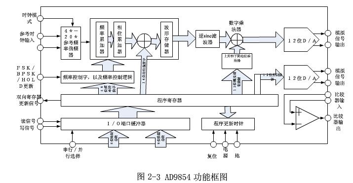
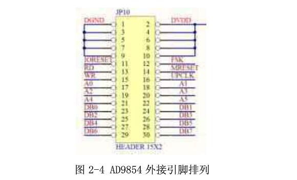
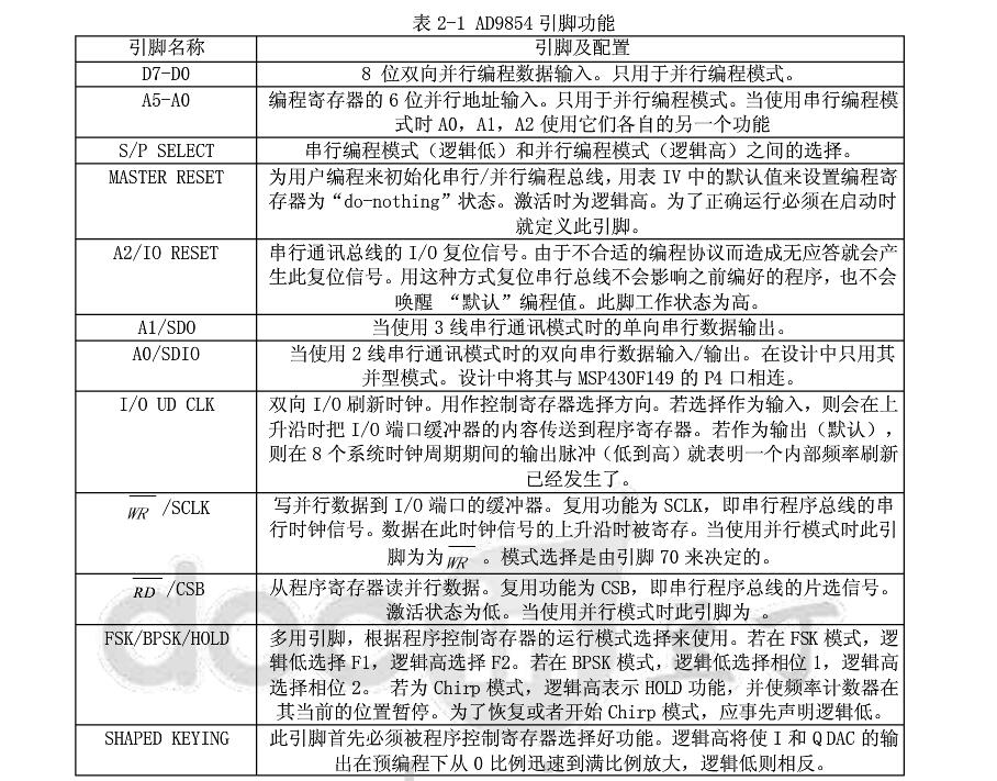
(1) To ensure reset after power-on, MASTERRESET is active high for at least 10 system clock cycles.
(2) Select the reference signal input mode. If single-ended input mode is used, REFCLKB should be connected to the power supply or ground. If multiple slices of the 9854 are used to generate multiple phase-correlated sine waves, the differential input mode should be used to reduce the phase error between the individual DDS reference clocks.
Select the data input method by setting the S/PSELECT pin to 1 for parallel and 0 for serial. We chose the parallel input method. The data is written to the 48-bit parallel register from the parallel input under the control of the WR signal and the UPDATE signal.
(3) AD9854 has two orthogonal outputs, IOUT1 and IOUT11; I0UT2 and I0UT22, this design fully uses two groups. The former only has a sine wave output and the other can only have a square wave output.
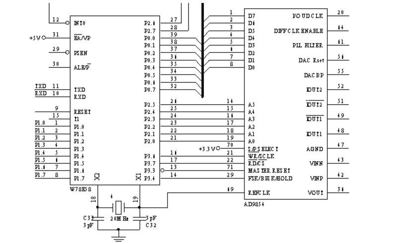
The SCM control chip used in the system is the W78E58 chip of Taiwan Winbond. It is a 51 series microcontroller compatible microcontroller and has 32KB of FLASH EPROM inside. Its one machine cycle is 4 times the oscillation cycle. The time for executing the same instruction is only 1/3 of the ordinary 8051 microcontroller, so the instruction operation is faster. In this article's design, the W78E58's reference clock is generated by a 20-MHz crystal oscillator, and it is also used as the input clock to the AD9854, and then it is multiplied by an internal multiplication circuit to achieve a 300-MHz system clock. AD9854 has 10MHz serial interface and 100MHz 8-bit parallel interface can be selected in two ways, here S/P SELECT (Pin70) pin is connected to high level, select parallel transmission mode. As shown in Figure 2, the P0.0 to P0.7 ports of the W78E58 are connected to the D0 to D7 ports of the AD9854 to transfer data information, and the P2.0 to P2.5 ports are connected to the A0 to A5 ports to transfer register address information, P3.6. , P3.7 and WR, RD are connected to the two pins to control the read and write operations, and the three parts form the parallel transmission control. For example, when the WR pin is set to a low level, the frequency control word is sent through the data port to the I/O buffer register. The internal refresh clock then writes the control word to the register at the specified address. In order to save the microcontroller I/O port and simplify the hardware circuit, this paper uses a matrix keyboard and combines software programming to implement dual function keys. The keyboard has a total of 16 keys, consisting of four lines P1.0~P1.3 and four lines P1.4~.P1.7. Including the number keys, unit keys and function keys, used to control the frequency, amplitude and function of the desired signal, the final output signal frequency, amplitude and other information through the LCD display. The display part adopts GXM1602NSL LCD module of Guoxian, its core is HD44780. The data transmission with the W78E58 adopts 8-bit parallel transmission and can display 32 lines of characters in two lines. HD44780 supports user-defined characters, so it can be programmed to display Chinese characters and digital information such as frequency, amplitude, and waveform. The communication interface (RS232) is also used in the design of this article to connect with PC. The control command of PC can interact with W78E58 through TXD (Pin10) and RXD (Pin11) to control the output of the signal source.
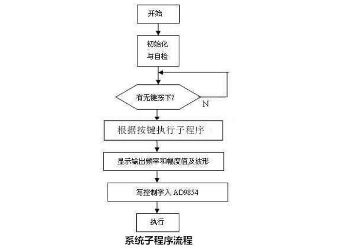
In the entire design of the instrument, a modular design method is used for the design of the system software. The system software consists of main monitoring software, keyboard display management module, peripheral interrupt management processing module, various functional modules, and data processing modules. After power-on reset, the instrument first enters the monitoring main program. Its task is to identify the command, interpret the command, and obtain the entry of the corresponding module that completes the command, which acts to guide the instrument into normal operation. The software of the system is designed in C language. Compared to assembly language, C language is convenient for the operation of the machine's underlying hardware, high degree of modularity, readability and portability.
When the following figure performs the initialization control of the AD9854, first, the MASTER RESET (Pin71) pin must be set high for 10 system cycles to _, and then the control word is written to the AD9854. Once set, the AD9854 will remain set until it is reset. The AD9854 stores a variety of control and status words associated with it through a register table with an address range of 00H to 27H. The user can communicate with this register table via I/O. The contents of the I/O buffer must be flushed to the register table under the action of the update pulse. This can achieve a good synchronization. The register tables 00H, 01H and 02H, 03H respectively store 14-bit phase control word 1 and phase control word 2, which determines the phase accuracy of the output signal programmable control, ie, the minimum phase is PMN = 360 degrees / 2 "* = 0.022 degrees.
The 04H~09H and 0AH~0FH units respectively store the 48-bit frequency control word 1 and the frequency control word 2, which determine the frequency accuracy of the output signal programmable control, that is, the minimum frequency is f MN=300X10*/2**=1.066X10 ~Hz. The five operating mode select words for the AD9854 are stored in Register Table 1EH. When the AD9854 operates in Chirp mode, the basic programming steps are as follows: (I) Write the initial frequency control word Wpc to the 48-bit FTWI (Frequency Tuning Word 1).
(2) Write the frequency step amount to 48-bit DFW (Delta Frequency Word). (3) Write the time step amount into 20-bit RRC (Ramp Rate Clock). (4) Update pulse refresh data. Part of the source program is as follows:
P2=0x04; Register address is 04HP0=0x2A; Output frequency is 50MHz
P3.6=0
P3. 6=1
P2=0x1F; Register address is 1FH
P0=0x86; operating mode is 011
P3.6=0
P3.6=1
. . . *..
P2=0x1E; Register Address is 1EH
P0=0x4F; The system clock is 15MHz, 20MHz, or 300MHz.
P3.6=0
P3.6=1
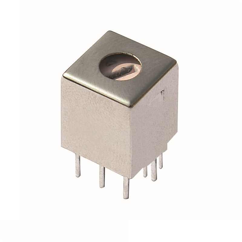
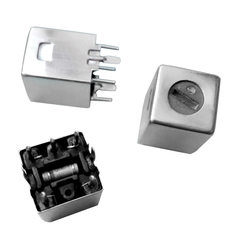
IFT Adjustable coils is a Power Inductor with widely range of inductance. It designed for different types of circuits and different application. Some of them with internal capacitor and some not. They widely used for Radio Receivers, AM FM Radios, Remote toy and Equipment and Wireless Communication System.
APPLICATIONS:
Compact fluorescent lamp
Television receiver
Radio cassette player
PC power supply
Monitor audio VCD DCD
UPS
The electronic apparatus
The noise rejection
Induction cooker etc.
SPECIFICATIONS:
High current capacity, electronic power inductor
Low core loss at frequency
High reliability, efficiency
Small packaged size
Operating Temperature: -30°C to +80°C
Electrical Specifications at 20°C
Model
IFT COIL
Brand
MGS
Material
Copper enamelled wire
Size and shape
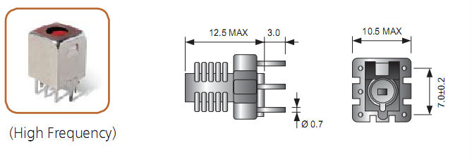
Can be made according to customer's request
Characteristics
RoHS compliant
Certification
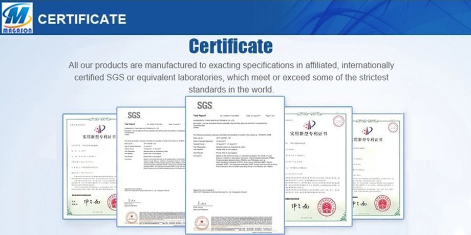
SGS Certification
Origin
China, Guangdong
Application
For Base Station, Power supply, Computer and also car audio, car electronics, DC-DC converter and telecommunication
Packaging
Can be packaged according to customer's request
Lead time
7 -10 days for mass production and 5 days for sample
Color
Customized
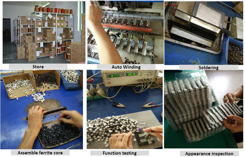

 Q: Are you trading company or manufacturer?
A: We are a customized factory.
A: Yes, we could offer the sample for free charge but do not pay the cost of freight.
A: Yes, Small quantity for trial order is available.
Ift Adustable Coil,Rf Tunable Coil,Ift Adjustable Coils,Ift Variable Inductor
Shaanxi Magason-tech Electronics Co.,Ltd , https://www.magason-tech.com
