As one of the most common electronic control measuring instruments used in electronic control measurement systems, signal generators are the basic instruments commonly used in industrial control, teaching and scientific research. Although various signal generators have gradually appeared in the market, they still cannot get rid of the shortcomings such as large size, many operation buttons, and high price, which brings inconvenience to the power system engineering personnel to go out to debug and repair the electronic control equipment. Considering many factors, it is necessary to develop a multi-function engine speed simulator with simple structure, convenient carrying and use. It can simulate and generate and output the speed (frequency) signal required for the site and the given current signal to debug the electronic control equipment (such as electronic governor) without starting the engine, which can greatly save The cost of the test (such as fuel cost, etc.), and the adjustment accuracy is high; the frequency of the external signal (ie, the speed signal of the on-site engine) can be detected in the state of being turned on, the numerical value display is performed, and the system is powered by the battery, so the multifunctional The successful development of the engine speed simulator will bring great convenience to the power system engineering technicians for on-site testing, and has high practical value and economic value.
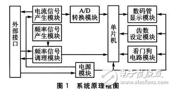
1 system overall design The block diagram of the multi-function engine speed simulator system is shown in Figure 1. It is mainly composed of power supply, frequency signal generation, frequency signal conditioning, frequency signal measurement, current signal generation, current signal measurement and single chip measurement display. The standard square wave signal with adjustable output frequency can be adjusted by the frequency adjustment knob, or the adjustable current signal can be output from 0 to 20 mA through the current adjustment knob, and displayed by the digital tube. In addition, it can detect the external input signal. frequency. Since the commissioning object is primarily an engine, speed measurement is another unique feature of the speed simulator.
The frequency signal generating circuit is shown in Figure 2.
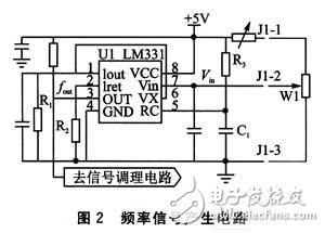
The core component of this circuit module is the LM331 voltage frequency conversion chip. It is an integrated chip with high performance and price produced by American NS company. It has the characteristics of large frequency adjustable range, low nonlinearity, high conversion precision, single power supply, etc. It realizes V/F function together with surrounding circuits. The frequency of its output signal can be calculated by equation (1):
Where: the unit of Vin is V, which represents the conversion voltage of U1; the unit of resistance of R1, R2, R3 is Q; C. The unit of capacitance is F; the unit of fout is Hz, which indicates the frequency value of U1 output. It can be seen that the signal frequency is proportional to Vin and has a good linear relationship. As long as the appropriate resistors and capacitors are selected and the performance of the varistor W1 is good enough, the output signal can be stabilized. The resistors used here are all metal film resistors.
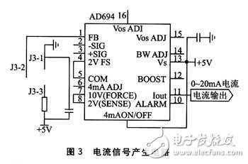
The current signal generating circuit is shown in Figure 3. The circuit module and the frequency signal generating module share a sliding varistor W1. The wiring is as follows: J3-1, J3-2, J3-3 are respectively connected to J1-1, J1-2, J1-3 in the frequency signal generating circuit, and the frequency and current adjustment are selected by the selection switch. Adjusting the value of the sliding varistor W1 enables current output of 0 to 20 mA. The core component chosen for this circuit is AD*. AD* is a monolithic voltage-to-current converter (hereinafter referred to as V/I). It converts the input voltage signal into a standard O ~ 20 mA current signal, which can be widely used for parameter transmission of pressure, flow, temperature and other signals, and control of some common equipment in valves, regulators and process control.
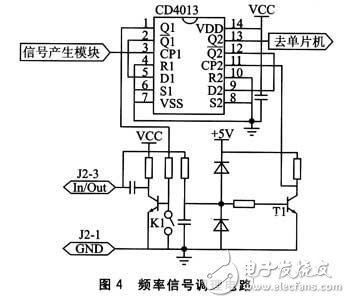
The frequency signal conditioning circuit is shown in Figure 4. Since the waveform generated by the frequency signal generating circuit is not very regular, it must be shaped by the CD4013, and finally collected by the MCU and displayed by the LED. If K1 is closed, the internal signal and ground are shorted, and an external pulse signal (such as a sinusoidal signal from a diesel magnetoelectric sensor) can be obtained because T1 and CD4013 will form a pulse width ratio of 1:1. The square wave can also be collected by the microcontroller. It should be noted that when the number of pulses is calculated by the MCU, the pulse signal after being divided should be considered, so the number of pulses counted in the software is doubled.
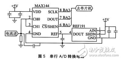
The serial A/D conversion circuit is shown in Figure 5. The O~20 mA current generated by AD* is converted into O~2. After the OV's analog voltage signal, it is connected to the CH0 and CH1 ports of the MAXl44. Because the analog signal voltage range is 0~2. OV, so the reference voltage of the MAXl44 can be set to 2.048 V, which can improve the conversion accuracy and facilitate the subsequent processing of the converted data. The 2.048 V reference voltage is available from REFl91.
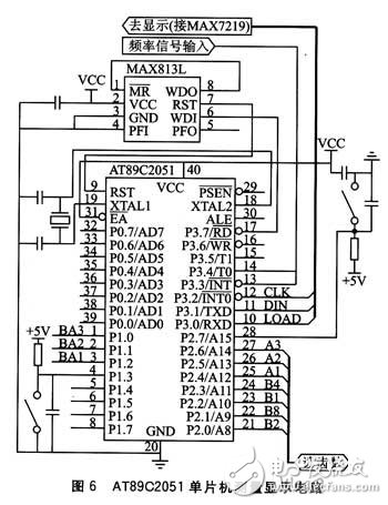
The core component of the measurement display circuit is the AT89C2051 microcontroller, and the circuit is shown in Figure 6. The reset watchdog adopts MAX813L to realize power-on reset and program monitoring (implemented in the program); the number of engine teeth is manually set according to the actual number of teeth, and is read by the single-chip microcomputer; MAX7219 is BCD decoder, display The driving function; the microprocessor uses Atmel's AT89C2051, which contains 2 KB of program memory, 128 bytes of data memory, 15 I/O ports and 2 timers, which is enough for the multi-function speed simulator.
The software flow of this system is shown in Figure 7. It includes frequency/speed measurement, serial A/D conversion value reading, numerical display and related processing.
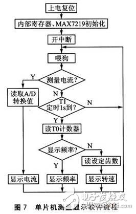
When the circuit is powered up, the MAX813L generates a reset signal to cause the microcontroller to reset. The program jumps to the start address 0000h, first initializes the internal registers and MAX7219, such as T0, T1, TMOD, and then interrupts T0, T1, and EX1. Feed the dog statement in the loop query, the time interval for feeding the MAX813L to the dog should be less than 1.6 s, otherwise it will generate a reset signal again, disturbing the normal operation of the program. Then, the P1.3 pin is detected. If it is low, the serial A/D conversion value reading program is executed; if it is high level, the MCU is triggered to interrupt on the falling edge of the signal, and the T1 timing and T0 counting are turned on. When T1 timing is 1 s, the T0 and T1 are turned off, and after the T0 value is read, the T0 and T1 are interrupted again, and the number of pulses is counted again. Then calculate (T0 value multiplied by 2), judge (when it is not more than 9999 or equal to 0, it is legal, and set the FLAG flag), then send to MAX7219, after it is decoded, it is displayed on the LED, and the frequency indicator light is on. Informing the user that the frequency value is displayed so that the knob W1 (see FIG. 2) is adjusted as needed to cause the generator to emit a desired frequency value signal, which is the principle of measuring the signal frequency; if the value is not legal, the LED will Do not display or display 0, then adjust W1 until it is legal. The frequency measurement and display procedure of the external signal is the same as before (the torsion switch needs to be screwed to the input file). If the P2.7 pin is low, the engine speed is measured. The previous frequency value is substituted into the speed formula (2):
n=(f·60)/k(2)
Where: n is the diesel engine speed (r/min), the factory is the measured frequency value (Hz), and k is the number of teeth of the engine speed measuring gear.
It can be seen that the MCU needs to read the tooth value, then calculate and judge (n is not greater than 9999), and send the LED display. It should be noted that the above is to first count the number of speed pulse signals in 1 s, and then calculate the speed by substituting formula (2). This measurement method is called frequency measurement. When the engine is running at low speed, the measurement cycle method is used: firstly measure the pulse average period, then use the division method to calculate the frequency value, substitute the speed formula to calculate, display and jump to the loop query, then use the division method to calculate the frequency value and substitute The formula of the speed formula is calculated. After the display, jump to the loop query and continue to query the timer interrupt.
3.2 Serial A/D conversion value reading software designSince the interface between the MAX144 and the microcontroller is very simple, only three I/O lines are needed, so the system uses the P1 of the microcontroller. O, P1.1, P1.2. The circuit adopts the internal clock mode. The MCU generates the serial clock by programming and reads the data according to the timing. The A/D converted data (16 bits) can be stored in the memory cells R2 and R3 inside the MAXl44. CHID can distinguish between CH0 and CH1 channels, then mask the upper 4 bits to get the actual A/D conversion data, and use ANLR3, 0FH to shield the upper 4 bits. After the end of the program, R3 is the upper 4 bits of the 12-bit data of A/D conversion, and the lower 8 bits of R2 are used, and then the program is converted by the program set in the MCU (OFFFH corresponds to 2.048 V, ie 20.48 mA; 0000H corresponds to 0 V, which is 0 mA), and the current value can be displayed.
ConclusionThe multi-function engine speed simulator uses fewer components, has lower cost, is easy to adjust, and is easy to implement. Through debugging, it is found that as long as the temperature coefficient of the RC element is low, the output frequency and current are quite stable, so the cost performance is high. The use of the multi-function speed simulator shows that it has good reliability, stable output and convenient carrying.
Pv Inverter,Pv System Grid Tie Inverter,Pv Solar Power Inverter,Solar Pv Inverter
GuangZhou HanFong New Energy Technology Co. , Ltd. , https://www.gzinverter.com
