The payment chip described here includes both a terminal integrated chip with SE and a separate card chip with SIM card as SE.
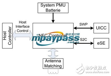
As shown in the figure below, several typical devices around the payment chip in the mobile terminal are drawn, and lines are used to describe the relationship between the devices.

(1) NFC Controller is the payment chip. The functions and structures have been introduced in the first two topics.
(2) The Host Controller in the mobile terminal is the terminal software for command control of the NFC Controller (NFC payment chip) in the terminal, which is generally implemented in the terminal operating system and implemented by the protocol stack, such as the Android+NFC Stack in reality, or iOS. +NFC Stack. The transport protocol between the Host Controller and the NFC Controller is determined by the NFC chip and the operating system, and is not a unified standard.
(3) System PMU Batterie is a battery or power supply device, generally a battery inside the phone, and supplies power to the NFC Controller.
(4) Anternna is an NFC radio frequency antenna placed in an NFC mobile phone terminal for receiving and transmitting non-contact signals. The size, shape and position of the antenna vary depending on the phone. The design of the antenna is the core element of the performance of the NFC mobile phone.
(5) eSE is an embedded security module for implementing contactless transaction logic, storing transaction data, downloading various electronic cards, etc. It is a module for security sensitive data and logic management, such as managing storage bank card balances and traffic card swiping. The number of times. These data are stored in the payment chip. In order to ensure the privacy of personal data, it is usually implemented in the SE module of the payment chip.
(6) UICC is a general term for SIM card or USIM card, similar to the role of eSE. The difference is that the eSE is placed in the payment chip, and the UICC is placed in the SIM card slot in the mobile phone. In addition to the eSE function, the UICC also has the function of performing mobile communication network authentication.

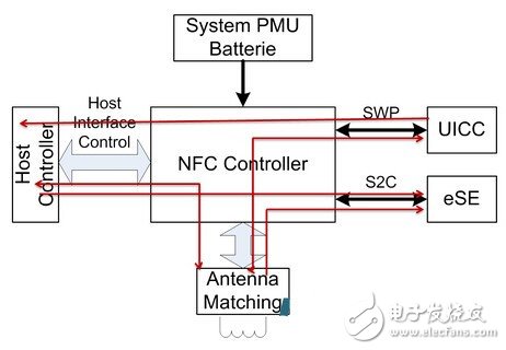
As shown in the figure above, the red line in the figure represents the signal relationship between different devices surrounding the NFC payment chip. There are three main types of signal working mechanisms for the security module and payment chip in the eSE form.
(1) For the NFC read mode, the NFC mobile phone is used as a POS or card reader. The Host Controller transmits signals through the NFC Controller and the antenna to read the external contactless card signals.
(2) For the NFC card mode, the NFC mobile phone is used as a non-contact IC card. The eSE transmits signals through the NFC Controller and the antenna, reads the external contactless card signals, and performs transaction processing.
(3) For the mobile phone application to directly access the eSE data, that is, the user views his bank card balance on the mobile phone, performs online storage, and downloads the electronic card. The Host Controller transmits signals to and from the eSE through the NFC Controller and eSE.
For the security module of the UICC form, several devices see the transaction basic principle similar to eSE, except that the transmission protocol used is different.
Among the working mechanisms of NFC payment chips, the most error-prone is also a place for skill:
(1) Concurrency processing techniques for reading and writing to the same device when several peripheral devices work together.
(2) The efficiency of signal transmission, which in turn affects the overall performance of NFC.
(3) Security control techniques for accessing security modules.
(4) For NFC several mode switching and automatic wheel training design skills.
(5) Quick positioning techniques for chip and software modules in question.
The development of NFC is the foundation. Developing NFC is a test of the differences between chip companies, COS companies, and software companies. At present, there are not many companies that can develop NFC in the world.
Tin Spray Pcb,Tin Spraying Circuit Board,Multilayer Tin Sprayed Circuit Board,Pcb Spray Tin Board
Shenzheng Weifu Circuit Technology Co.Ld , https://www.wfcircuit.com
