
Author: Kevin Smith, Silicon Labs
Hello, welcome to Timing 101 seconds to understand the technical series of clock series, this series of articles for the special column of Silicon Labs (also known as " core technology " ) clock technology experts. Our goal is to introduce and summarize the technical topics in the application of timing components or ICs (also known as " clock chips " ). The clock chip transmits frequency and phase information through a clock waveform, and in some cases can packetize timing information.
In this article, we will introduce a common set of measurement conditions. When the jitter attenuator is initially used, the test results may be unexpected. First, review some of the necessary background materials, then show the problem and its root cause, and finally propose improved test settings.
Introduction to jitter and phase noiseIn short, a clock is a periodic signal with a digital signal level for sampling data in a synchronous digital system. In other words, the clock provides the " heartbeat " or rhythm required to sample and sequence the data in a synchronous digital circuit or system . They are usually, but not always, at 50 % or nearly 50 % duty cycle.
The ideal clock will provide the perfect specified frequency and phase to optimize this process. However, the actual clock has timing jitter, which can be defined as a short-term change in the clock edge and its ideal value. One reason for concern about clock jitter in synchronous digital systems is that it can enter timing margins, which can affect the reliability and effectiveness of the data.
There is also a frequency domain corresponding to jitter: phase noise. Phase noise measures the random short-term phase fluctuations of the clock. This indicates the purity of the clock.
In short, there is a map of L ( f ). The relationship between the noise power of the one-phase modulation sideband and the carrier power is shown in the case of carrier frequency offset. For example, at 100kHz is -70dBc / Hz, in the 20MHz to -150dBc / Hz. The dBc / Hz unit is the power ( dB ) of the carrier power relative to the bandwidth per Hertz . Phase noise is typically measured using a phase noise analyzer or a spectrum analyzer with phase noise options.
Usually shown on the same graph is a non-random short-term clock phase fluctuation called spurs or spurious . These spurious are represented as discrete components in dBc .
As with other system analyses, we often find it easier to understand clock devices and clock distribution networks or clock trees in the frequency domain.
The role of the jitter attenuatorIt is not uncommon to have to use, or at least start with, a clock that is relatively noisy or jittery. These may be for a number of reasons. For example, when the clock is:
·       Recover from serial data stream
·       From noise-intensive ICs such as FPGAs or noisy PC boards
·       Derived from TCXO or OCXO with good drift specifications, otherwise jitter will occur
·       " Gap " means that the edge is missing for synchronization purposes
In this case, we need a specific type of clock device, jitter attenuator or " jitter cleaner " to attenuate or minimize phase noise and exceed the offset frequency of interest. The resulting output clock is then distributed to devices that need to improve jitter performance.
Jitter attenuators are characterized in that they are essentially narrow-band phase-locked loops ( PLLs ) with a " low-pass " jitter transfer function . This is the jitter component of these devices where the attenuation frequency is greater than the PLL loop bandwidth ( BW ). Modern jitter attenuators typically have a programmable loop BW ranging from 0.1 Hz up to 1 or a few kHz .
In contrast, another type of clock chip, the clock generator, is a wideband PLL that is primarily used for clock multiplication from low jitter sources . These devices typically have a fixed loop bandwidth of approximately 100 s kHz to 1 MHz .
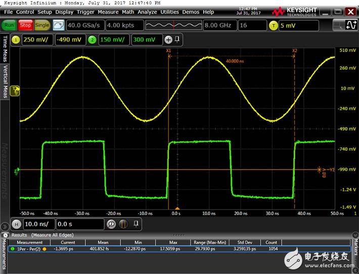
Measuring problemSo the question is coming? Customers often contact us and write down a clock chip like we are testing you, and compare the output clock to the input clock, but the jitter is large. We will always find that the test setup boils down as follows: The oscilloscope is triggered by the jitter input clock. Â Â
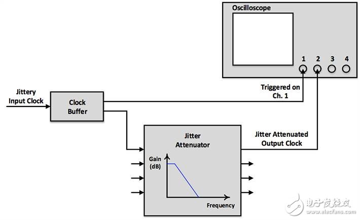
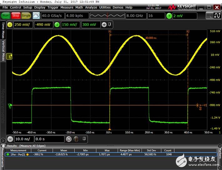
The results usually look similar to those shown below. In this example, the jitter attenuator is a Si5347 with a loop BW = 100Hz . The yellow trace at the top is the input clock, which is a 25 MHz sine wave from the signal generator with a 1 kHz FM , 100 Hz offset. The green trace at the bottom is the output clock, just to keep it simple, it is also 25 MHz .
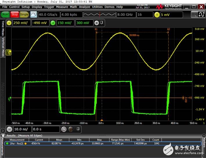
The output clock should be less jittery, is the jitter attenuated? This is the case with a jitter-attenuated clock.
Considering the measurement setup described earlier, there must be three factors to observe this obvious problem:
1. Â Â Â Â Input clock jitter.
2. Â Â Â Â The output clock jitter is not large. In other words, the jitter attenuator is doing its job.
3. Â Â Â Â The output clock is triggered by the input clock by comparison with the input clock.
Now you should be able to recognize the basic issues, even if they are hidden in more complex applications.
Note that if you trigger on the output clock, the input clock will appear to be very jittery. as follows. Which clock appears to be jitter is just a matter of triggering the angle of view. This particular range measurement is not decisive without knowing which clock is more unstable.
You can get information about the real situation of this particular test configuration through the loop bandwidth of the jitter attenuator. Try to narrow and expand the BW and then observe the results within the range.
Assuming there is a dithered input clock, you should normally see that widening the BW causes the output clock to show less jitter than the input clock. This is because widening the BW means that the PLL will track more input clocks, jitter and others. In Figure 4 below, the loop width of the Si5347 has been expanded to 4 kHz . There is essentially no jitter attenuation, and the output clock does not show jitter compared to the input clock.
Conversely, shrinking the BW will make the output clock more jittery than the input clock. This is because the narrower loop BW corresponds to more jitter attenuation. Ironically, the jitter attenuator in this test configuration is very successful, which is the root cause of the problem. If the output clock is only tracking the input clock, the trigger source will be irrelevant. In the figure below, the loop width of the Si5347 is reduced to 100 Hz .

A jitter-attenuated clock is usually different from its jittered input clock, scaling above and beyond any frequency. If the spectrum changes significantly, it should be relatively obvious when measuring and comparing the phase noise of each clock. However, as mentioned earlier, this requires specialized equipment such as phase noise analyzers or spectrum analyzers with phase noise options.
Third party arbitrationIf you have a range, what better way to compare jitter input and jitter attenuation output clocks at the same time? Find the third party to the arbitration. In other words, an integer associated with the jitter reference clock is found or generated and synchronized with the input and output clocks. It is then used as a reference for the triggering of the input and output clocks. See the revised test setup diagram in the figure below. Now you can clearly compare the jitter of the input and output clocks simultaneously in the time domain.
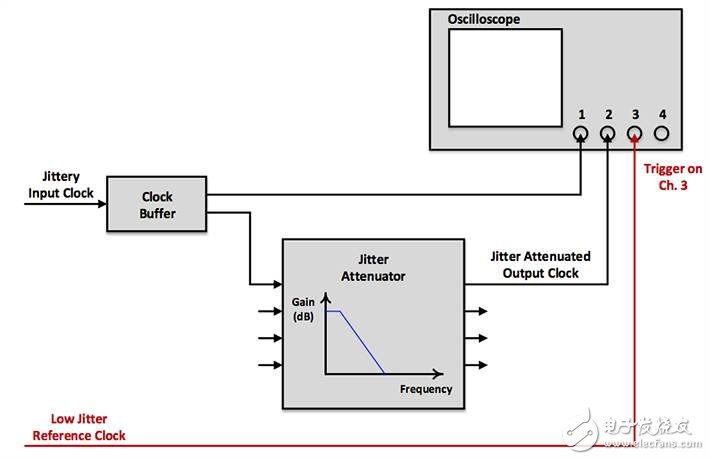
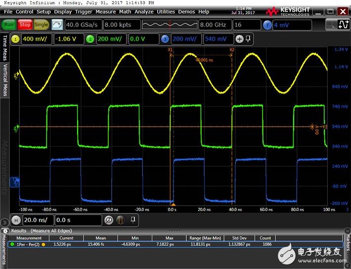
Here are a few sample diagrams where all oscilloscope traces are 25 MHz as previously described . The yellow trace at the top is the jitter (frequency modulation) input clock, and the green trace in the middle is the output clock of the jitter attenuator. The blue trace at the bottom is the new low jitter reference clock used as a trigger. First, in the figure below, the jitter attenuator has a loop BW of 4 kHz and the output clock is as jittery as the input clock.
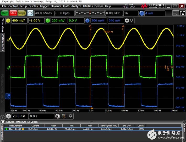
In the second case, in the figure below, the jitter attenuator's loop BW is 100 Hz and the output clock jitter is much smaller. In this particular example, when the loop BW is reduced from 4 kHz to 100 Hz , the standard deviation of the jitter-decay clock period from the period jitter drops from 8.2 ps to 1.1 ps .
China Top Laptop Stand Ergonomic, Ergonomic Flexible Laptop Stand, Adjustable Laptop Computer Stand Manufacture in Shenzhen. Shenzhen Chengrong Technology Co.ltd is a high-quality enterprise specializing in metal stamping and CNC production for 12 years. The company mainly aims at the R&D, production and sales of Notebook Laptop Stands and Mobile Phone Stands. From the mold design and processing to machining and product surface oxidation, spraying treatment etc ,integration can fully meet the various processing needs of customers. Have a complete and scientific quality management system, strength and product quality are recognized and trusted by the industry, to meet changing economic and social needs .

Laptop Stand Ergonomic,Ergonomic Flexible Laptop Stand,Adjustable Laptop Computer Stand,Desktop Foldable Aluminum Laptop Stand
Shenzhen ChengRong Technology Co.,Ltd. , https://www.laptopstandsuppliers.com