In embedded systems, the application of MCU and DSP is very common, and analog signals and various digital signals exist simultaneously. Traditionally, engineers used oscilloscopes and logic analyzers for testing and verification. However, due to the complexity of the mixed signal, it is very difficult to achieve synchronous triggering of various signals. With the advent of a hybrid signal oscilloscope (MSO), engineers found that embedded design debugging is much easier.
MSO is a hybrid test instrument that combines all the measurement capabilities of a digital storage oscilloscope (DSO) with some of the measurement capabilities of a logic analyzer, and allows the oscilloscope and logic analyzer to share trigger circuits so that they can be triggered simultaneously. The waveform is displayed and refreshed simultaneously. With the MSO, multiple time-aligned analog and digital waveforms as shown in Figure 1 can be seen on the same display, and the delay between the oscilloscope channel and the logic channel is almost negligible ("30ps").
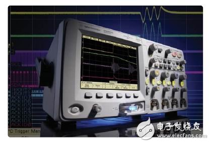
Figure 1: Agilent 6000 Series Mixed Signal Oscilloscope.
MSOs often lack the complex analysis capabilities of dedicated logic analyzers (such as disassembly, etc.) and the large number of logical channels; the relative simplicity of MSOs also allows them to avoid the complex operations of dedicated logic analyzers. In fact, one of the main advantages of MSO is its usage model. The use of MSO is almost the same as using an oscilloscope. Since the MSO is highly integrated, it is much easier to use than using two separate instrumentation schemes. A good MSO should have a friendly user interface that provides fast waveform update rates, and the instrument operates much like an oscilloscope rather than a logic analyzer.
Embedded "chirp" design
Figure 2 is a block diagram of the embedded “chirp†product developed by SoluTIons Cubed for an embedded industrial application. At the heart of this mixed-signal embedded product is the MICROChip PIC18F452-I/PT microcontroller, which implements an internal 16-bit instruction set. Since this special MCU has an internal bus structure and includes an embedded ADC, the mixed-signal device and corresponding peripheral circuits are the most suitable for designing and debugging with MSO. Although understanding this particular design is not necessarily closely related to the reader's specific design application, we will continue to explain the work of the system to give the reader an idea of ​​how MSO can be used for this type of mixed-signal measurement application.
The ultimate goal of this design is to generate "chirp" signals of various lengths, shapes, and amplitudes based on various analog, digital, and serial I/O input conditions (the signal is an RF pulse analog signal that includes a specific number of cycles, Aerospace is often seen in defense and automotive applications. The MCU simultaneously detects the following three analog and digital inputs to determine the analog characteristics of the output chirp signal to be generated:
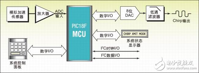
Figure 2: Mixed-signal embedded design that produces analog “chirp†outputs based on analog, digital, and serial I/O.
1. Use one of the MCU's parallel digital I/O ports to monitor the state of the user's control panel to determine the shape of the resulting output chirp signal (sine, triangle, or square).
2. Monitor the output level of the accelerating analog input sensor by the input of an ADC on the MCU to determine the amplitude of the resulting output chirp signal.
3. Use the dedicated I2C serial I/O port on the MCU to monitor the status of the serial I2C communication link to determine the number of pulses generated in the output chirp signal. This I2C communication input signal is generated from another intelligent subsystem component of the embedded design.
Based on the three input states of analog, digital, and serial, the MCU continuously outputs parallel signals to an external 8-bit DAC to generate analog chirp signals of various amplitudes, shapes, and lengths. The unfiltered DAC output step signal is fed into an analog low-pass filter where the signal is smoothed and noise is reduced. This analog filter also introduces a predetermined amount of phase shift for the output signal. Finally, the MCU generates a parallel digital output through an additional digital I/O port to drive an LCD display that displays system status information.
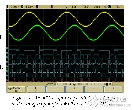
Figure 3: The MSO captures the parallel digital inputs and analog outputs of the DAC controlled by the MCU.
Enable and debug embedded "chirp" designs with MSO
In this application design, the first step in designing an MCU is to configure the appropriate number of analog and digital I/O ports for the I/O of the MCU. You have to trade off the number of analog I/O ports and digital I/O ports in this special microcontroller from MicroChip.
Before attempting to encode an MCU to monitor various inputs and output signals that produce the specified final requirements, we decide to first generate test code that enables a certain part of the embedded design to be verified before adding interactive complexity. It works correctly and signal integrity. The first part of the circuit that is enabled and debugged is the external output DAC and analog filter. To verify that the circuit and internal firmware are working correctly, we originally coded the MCU to produce a fixed-amplitude continuous and repeated sine wave regardless of the input control state signal condition.
Figure 3 shows the screen image of the MSO, which is the continuous digital output (blue trace below) used to capture the digital I/O port of the MCU that drives the external DAC digital input. In addition, we can see the time-aligned converter step-wave output (the yellow trace above) and the analog filtered output signal (the green trace in the middle). The output level of these specific signals is low, only 4 bits (16 levels) of 8-bit DAC (maximum 256 levels), we can easily observe the unfiltered step wave output characteristics of the converter on the oscilloscope .
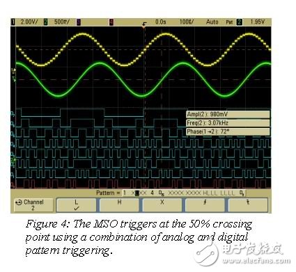
Figure 4: Using a combination of analog and digital pattern triggering, the MSO triggers at the 50% crossover point.
When the DAC output reaches its maximum output level (center of the screen), we set this particular acquisition to the trigger state. Triggering of a conventional oscilloscope at this specified point is not possible because the oscilloscope triggers a jump that requires an edge—the oscilloscope cannot trigger on a “wave top†with a range of signals. To trigger at this point in the output signal, we set up a simple one-level pattern trigger condition based on the DAC's (MCU I/O port output) digital input signal, which is external to the converter. The highest output analog level is consistent. To trigger at a certain point in the waveform, we send a parallel binary pattern of "HHHL LHHL" for triggering. Since the MSO uses a “qualified†pattern trigger, the oscilloscope always triggers at the beginning of the specified pattern and never triggers at an unstable transition because the oscilloscope requires that the logic level be at least 2ns stable, then only Triggered when a stable pattern is fed. Note that for some mixed-signal measurement solutions, you can trigger whenever there is a specified pattern trigger condition. This means that they are likely to be triggered in the intermediate state of the pattern or in the transition state of the transition. Without a "qualified" pattern trigger, the result will be an unstable trigger.
Figure 4 shows a one-shot setup scenario where the MSO provides a precise trigger at the 50% output level of the DAC. To implement such a trigger, in addition to the analog trigger condition, we also utilize the trigger pattern that is triggered on the parallel digital input signal. It should be remembered that not all MSO® mixed-signal measurement solutions allow mixed-signal triggering of analog and digital trigger conditions. However, for two analog output conditions of the same level (50% rise level and 50% fall level), the trigger level required for the trigger coincides with the rise or fall point is slightly larger than the 8-bit input pattern. By additionally limiting the level on analog channel 2 to the "low" level, the oscilloscope can use a combination of analog and digital pattern triggers to trigger on the desired phase (the analog signal is considered above the analog trigger level) "High" is considered "low" when it is below the trigger level).
The automatic parameter measurement is also shown in Figure 4, including the amplitude, frequency, and phase shift of the filtered output signal associated with the DAC step wave output.
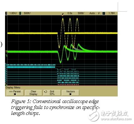
Figure 5: Edge triggering of a traditional oscilloscope cannot synchronize chirps of a specific length.
After starting and verifying that the external DAC and analog filter circuits are operating correctly, the next step in the design startup process is to generate a specified number of non-repetitive sine wave pulses (chirp) based on the serial I2C input. Figure 5 shows the resulting overlap of different lengths of chirp (infinite persistence) using a standard oscilloscope edge trigger. It is impossible to trigger the specified length chirp by the edge trigger of the traditional oscilloscope.
Using the MSO's I2C triggering capability, the oscilloscope can synchronize the capture under specific serial input conditions to instruct the MCU to produce an output chirp of the specified length (number of pulses), as shown in Figure 6 and Figure 7.
Figure 6 shows the MSO's ability to trigger a chirp signal with only 3 cycles long using I2C triggering on a specific serial address and data content. Figure 7 shows the triggering capability for a chirp with a length of only 1 cycle. Data channels D14 and D15 (the two blue digital traces above) are defined as the I2C clock and data input trigger signals, respectively. In fact, we can specify that any of the 16 digital channels and 2 to 4 analog oscilloscope channels are continuously triggered on these 2 serial input signals. When monitoring serial input and analog output signals, D0-D7 is set to detect the DAC input (MCU output) signal (eight blue traces and read digital traces below), as shown in Figure 6 and Figure 7.
Although not shown in the figure, we can set the other analog channels of the oscilloscope to synchronously detect, acquire, and trigger the MSO based on the other analog input signals of the analog acceleration sensor used to determine the amplitude of the output signal. In addition, we can take advantage of unused MSO digital channels to monitor and/or further enable high quality triggering of CNC panel inputs or LCD output driver signals.
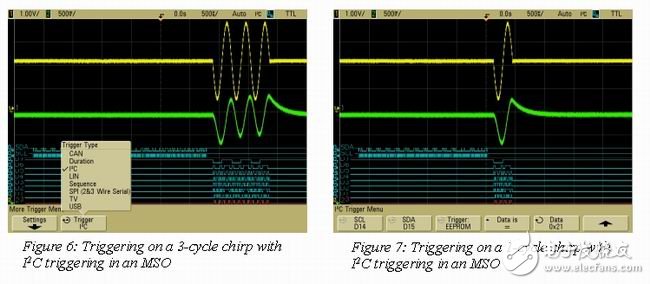
Figure 6: Triggering a 3-cycle long chirp signal with I2C in the MSO. Figure 7: Triggering a chirp signal with only 1 cycle long with I2C in the MSO.
ZGAR PCC
ZGAR electronic cigarette uses high-tech R&D, food grade disposable pod device and high-quality raw material. All package designs are Original IP. Our designer team is from Hong Kong. We have very high requirements for product quality, flavors taste and packaging design. The E-liquid is imported, materials are food grade, and assembly plant is medical-grade dust-free workshops.
From production to packaging, the whole system of tracking, efficient and orderly process, achieving daily efficient output. We pay attention to the details of each process control. The first class dust-free production workshop has passed the GMP food and drug production standard certification, ensuring quality and safety. We choose the products with a traceability system, which can not only effectively track and trace all kinds of data, but also ensure good product quality.
We offer best price, high quality Vape Device, E-Cigarette Vape Pen, Disposable Device Vape,Vape Pen Atomizer, Electronic cigarette to all over the world.
Much Better Vaping Experience!


E-Cigarette Vape Pen,Disposable Device Vape,Vape Pen Atomizer,Latest Disposable E-Cigarette OEM vape pen,OEM electronic cigarette
ZGAR INTERNATIONAL(HK)CO., LIMITED , https://www.zgarpods.com
