A through-wall radar is a radar system that can penetrate non-metallic walls and detect, track, and locate people or objects behind the wall. It generally uses an ultra-wideband stepping system. The through-wall radar system built by our laboratory requires a signal source in the l~2 GHz band. According to system bandwidth and system parameters such as spurs and phase noise, the author uses DDS+PLL mixed frequency synthesis technology, and makes full use of AD9858 and other high integrated chips to design a frequency synthesizer that can meet the system signal source output requirements.
1 System principle and structureThe basic principle of the DDS+PLL frequency synthesizer is to excite or insert a PLL with a low frequency, high resolution DDS frequency, and then combine the advantages of both to produce a high quality signal source.
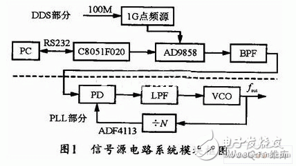
This paper uses the DDS excitation PLL scheme to meet the system requirements. The system uses a highly stable frequency source as the system reference clock; and writes the frequency control word and phase control word to the DDS internal register under the control of the single-chip microcomputer, and then the DDS generates an analog sine wave output that can be programmed and controlled by frequency and phase. And the output of the DDS is used as the reference signal of the PLL, and finally the frequency division ratio N of the frequency divider is set according to the signal frequency required by the through-wall radar system, thereby obtaining the system output signal. The signal source realized by such a scheme has a higher frequency and a faster frequency conversion speed, and the high performance of the integrated chip such as the AD9858 enables the system to meet the requirements in terms of spurs and noise.
2 circuit designThe circuit design of this system is mainly divided into two parts: DDS module and PLL module. The system block diagram is shown in Figure 1.

2.1 DDS module circuit design
The system guarantees high frequency resolution and good reference source performance by DDS, while the PLL increases the frequency output and filters out the DDS output spurs. The frequency hopping mode is realized by controlling the DDS and PLL.
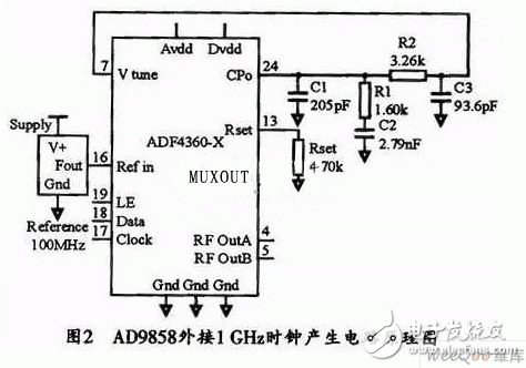
The external 1 GHz clock point source of the AD9858 can be generated using the ADF4360_2 and can be simulated using ADIsimPLL. The basic circuit schematic is shown in Figure 2. The reference clock of the ADF4360_2 uses a 100MHz active crystal oscillator. The actual circuit design needs to be filtered and then connected to the Ref port. The output frequency is 2 GHz and can be set to a divide-by-2 output. It can also be set to a divide-by-2 input on the AD9858 chip.

Control The AD9858 mainly uses the special function registers SFR, FIASH and external memory interface EMIF of C8051F020. The SFR provides control over the resources and peripherals of the CIP-51 and the data exchange between the CIP-51 and these resources and peripherals; FLASH is the internal memory of the C8052F020, which can be programmed via the JTAG interface; the external memory interface EMIF The royal access to the off-chip memory. The process of configuring EMIF is as follows:
(1) Select EMIF to the low port (P3, P2, Pl, P0) or high port (P7, P6, P5, P4);
(2) Selecting a multiplexing or non-multiplexing method;
(3) Select the memory mode (only use on-chip, only off-chip; without block selection, slice selection, etc.);
(4) setting the timing with the off-chip memory;
(5) Select the output mode of the relevant port (registers PnMDOUT and P740UT).
2.2 Basic Principles and Performance of AD9858
DDS is a digital frequency generator based on a lookup table. When the DDS device is operating, its frequency control word K is accumulated in each clock cycle, and the remaining phase accumulators are accumulated once, and the obtained phase value is obtained.
(O ~ 2Ï€) in each clock cycle, the sinusoidal lookup table ROM is addressed in binary code, and the phase information is converted into a corresponding digitized sinusoidal amplitude value, and the digitized waveform of the ROM output is passed through a digital-to-analog converter (DAC). After that, it is used to realize the conversion of the digitized signal to the analog signal. Finally, the stepped sequence wave of the DAC output is smoothed by a low-pass filter (LPF) to obtain a pure sinusoidal signal.
The AD9858's 10-bit digital-to-analog converter can operate up to lGsps and is capable of generating frequency-step-variable analog output sine waves up to 450MHz with fast frequency modulation and subtle frequency resolution (32-bit frequency resolution). The AD9858 has an integrated charge pump (CP) and phase detector (PFD) for on-chip analog mixing of high-speed DDS and phase-locked loops (PLLs), as well as DDS, PLL and mixers. .
The AD9858 has both single and sweep modes of operation. In mono mode. The AD9858 generates a single-frequency output signal that is controlled by the internal register FTW. The relationship between the output frequency and the system clock can be determined by the following formula:
![]()
For the AD9858, N=32. It can be seen that the frequency can be changed arbitrarily by changing the FTW. It is also possible to select a frequency value stored in the register in advance by an external pin to achieve fast frequency hopping.
In the sweep mode, the user needs to set the frequency sweep initial value, frequency step value and frequency step by frequency control word (FTW), frequency conversion control word (DFTW), frequency slope control word (DFRRW). Time, thus achieving sweeping.
Careful consideration should be given to the input and output frequency bands when designing DDS: when the output frequency is close to fc/n (where n=3, 4, 5, 6, 7; fc is the clock frequency of DDS), the spurs generated by the difference frequency signal It is close to the output frequency, so that it cannot be filtered by the filter. This narrow-band spurs will continue to deteriorate after multiplication, which will seriously deteriorate the spurious performance. Therefore, the DDS output band cannot be used close to and across fc/n. Frequency (where n = 3, 4, 5, 6, 7). The input frequency of the DDS in this system is 1 GHz. Therefore, the output frequency band is 50 to 100 MHz. This way, there will be no large spurs near the output channel.
2.3 PLL module design
Fork Type Connecting Terminals
Fork Type Connecting Terminals,Terminals,Connecting Terminals
Taixing Longyi Terminals Co.,Ltd. , https://www.longyicopperlugs.com
