ITO is a transparent electrode material with high conductivity, high visible light transmittance, high mechanical hardness and good chemical stability. At present, the ITO film is mainly used to improve the light-emitting efficiency of the LED.
What is the Burstein-Moss effect?
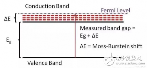
Burstein-Moss effect: When the semiconductor is heavily doped, the Fermi level enters the conduction band, and the intrinsic light absorption edge moves toward the high energy direction.
In ordinary doped semiconductors, the Fermi level lies between the conduction band and the valence band. When the n-type doping concentration rises, due to the accumulation of electrons in the conduction band, the Fermi level will slowly be deduced into the conduction band (it can be simply understood as water (which can be simply understood as ice (Fermi level)). Electronic) push to the high position).
What is a precursor (precursor)?The precursors refer to specially processed materials used to synthesize and prepare other substances.
Guide
A few days ago, researchers from Sun Yat-Sen University invented a process for preparing indium tin oxide film (ITO) in LED structures using metal organic vapor deposition (MOCVD). This method can effectively enhance the transparent and conductive properties of UV LEDs.
Generally, UV LEDs are divided into three types: UVA, UVB, and UVC according to wavelength. At present, it is mainly used in the fields of water purification, biological sterilization and disinfection, medical diagnosis and treatment, and ultraviolet treatment.
research processAlthough ITO is a transparent conductive layer material in the visible spectral region, the transparency of ITO will gradually decrease in the ultraviolet region.
Therefore, the Sun Yat-Sen University team managed to use MOCVD technology to broaden the width of the optical band gap to 4.7 eV. The wavelength of the photons excited by the band gap is exactly in the ultraviolet region (364nm).
Generally, UV LEDs are divided into three types: UVA, UVB, and UVC according to wavelength. At present, it is mainly used in the fields of water purification, biological sterilization and disinfection, medical diagnosis and treatment, and ultraviolet treatment.
Figure 1 Optical and electrical characteristics of ITO film in 90nm MOCVD process
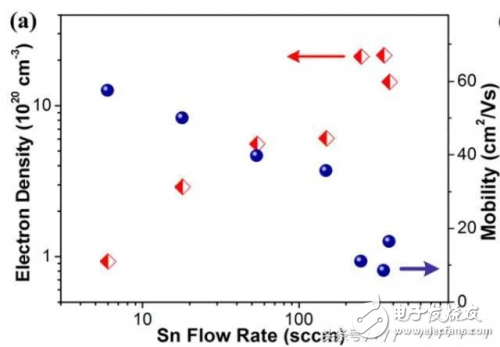
(A) The influence of Sn flow rate on electron density and mobility
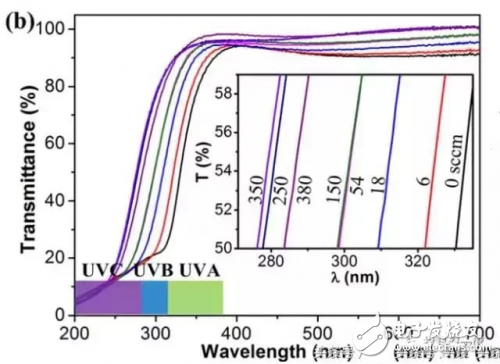
(B) UV visible light transmittance in ITO film in MOCVD process and different tin flow rate.
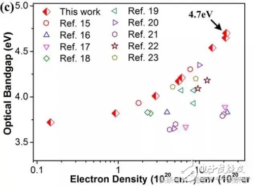
(C) Comparison of ITO optical band gaps under different processes
The Sun Yat-Sen University team first used MOCVD technology (the growth environment temperature is about 500°C) to grow a 90nm ITO film on the sapphire surface. The precursors are trimethyl indium, tetrakis-dimethylamino tin, and oxygen. Argon mixed gas. The surface of the finally obtained material has particles in the shape of a pyramid (100) and a triangle (111).
After many research experiments, the researchers found that controlling the addition rate of the precursor body at 350 cubic centimeters per minute will achieve the highest free electron density (2.15x10²¹/cm3). At the same time, the optical band gap will reach 4.70eV. Usually the electron density of indium oxide (In2O3 without precursor) is only 1.47x10¹⁹/cm3, and the band gap is 3.72eV.
This difference in band gap width is mainly due to the influence of the Burstein-Moss effect. At this time, part of the free electrons are concentrated in the low conduction band (conducTIon band), so more photon energy is needed to excite the electrons from the valence band. come out. The researchers said that using this method to broaden the forbidden band width by 0.98eV, this increase of close to 1eV is extremely rare.
At the same time, the researchers also believe that the MOCVD process can improve the problem of lattice distortion (Lattice distorTIon), which is a cause of the narrow band gap of ITO.
Figure 2 The epitaxial structure of the LED
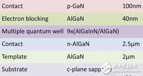
Generally, compared to the MOCVD process, the magnetron sputtering process can also produce a 120nm transparent conductive layer. This process uses a mixture of tin oxide (SnO2) and indium oxide (In2O3), and its composition ratio is controlled at 1:9. The magnetron sputtered material needs to be annealed at 550°C and placed in a nitrogen atmosphere for 5 minutes.
By analyzing the spectrum, the peak wavelength of the UV LED at this time is 368nm (Figure 3a). At this wavelength, the transmittance of the ITO film in the magnetron sputtering process is 86%, and the transmittance of the ITO film in the MOCVD process is 95%. However, the resistivity of the ITO film in the magnetron sputtering process is lower than that of the ITO film using the MOCVD process, and the contact resistance of the magnetron sputtering process is larger.
Figure 3 Optical and electrical characteristics of 120nm MOCVD ITO film and magnetron sputtering ITO film
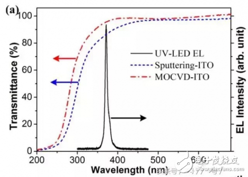
(A) Conductivity of 120nm MOCVD ITO film and magnetron sputtering ITO film on sapphire substrate, and LED emission spectrum using MOCVD ITO film
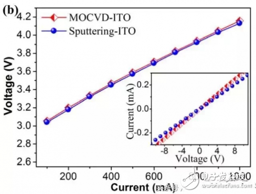
(B) LED current and voltage characteristic curve of ITO film with two processes
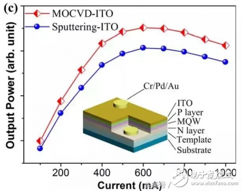
(C) Characteristic curve of output power and current
in conclusionThe ITO film of the MOCVD process can increase the output power by 11.4% and 14.8% under the current conditions of 350mA and 600mA respectively (Figure 3c). After multiple sample tests, the average working voltage is 3.45V at a working current of 350mA. The LED current and voltage curves of the ITO film using the above two processes are almost the same (Figure 3b).
ZGAR Vape Pods 1.0
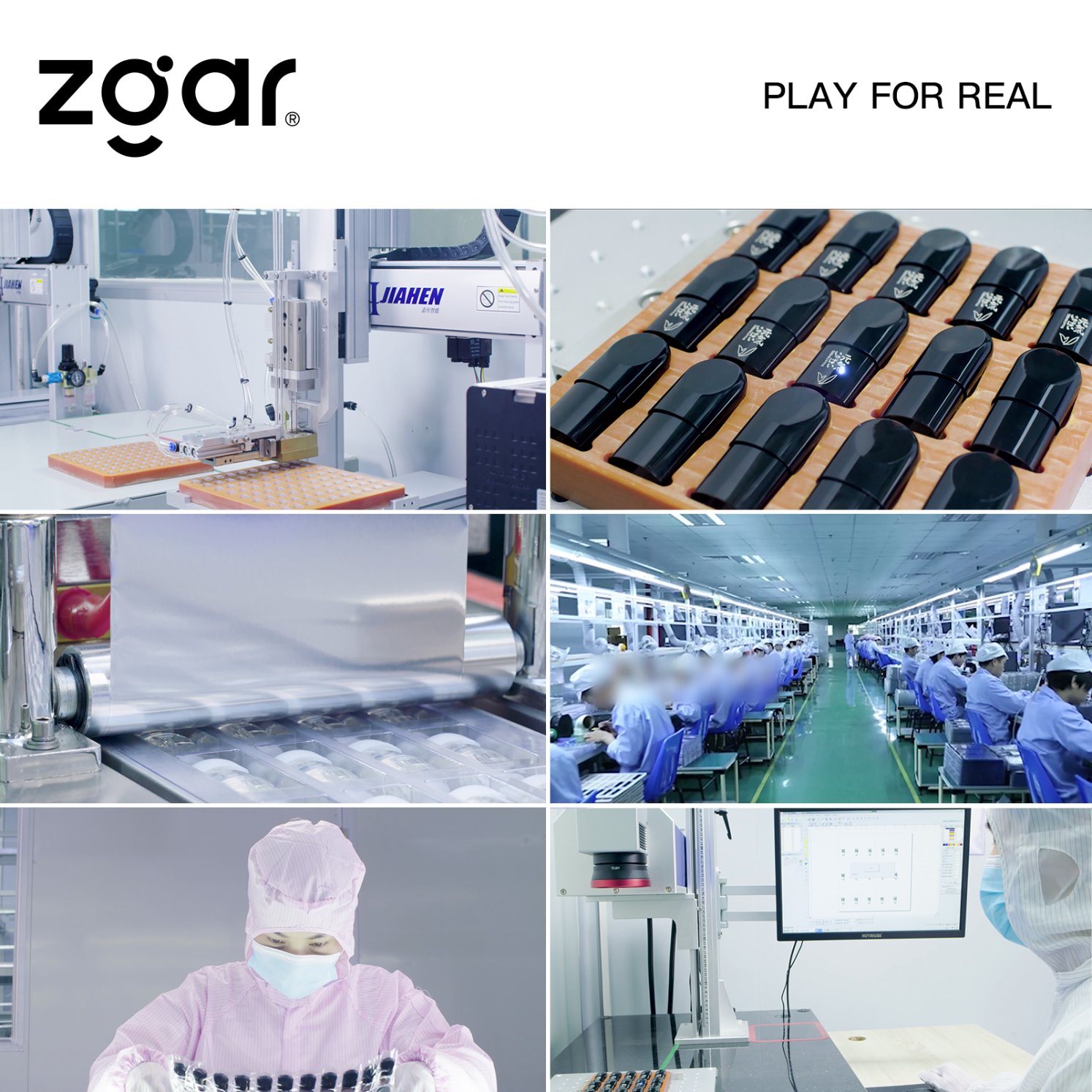
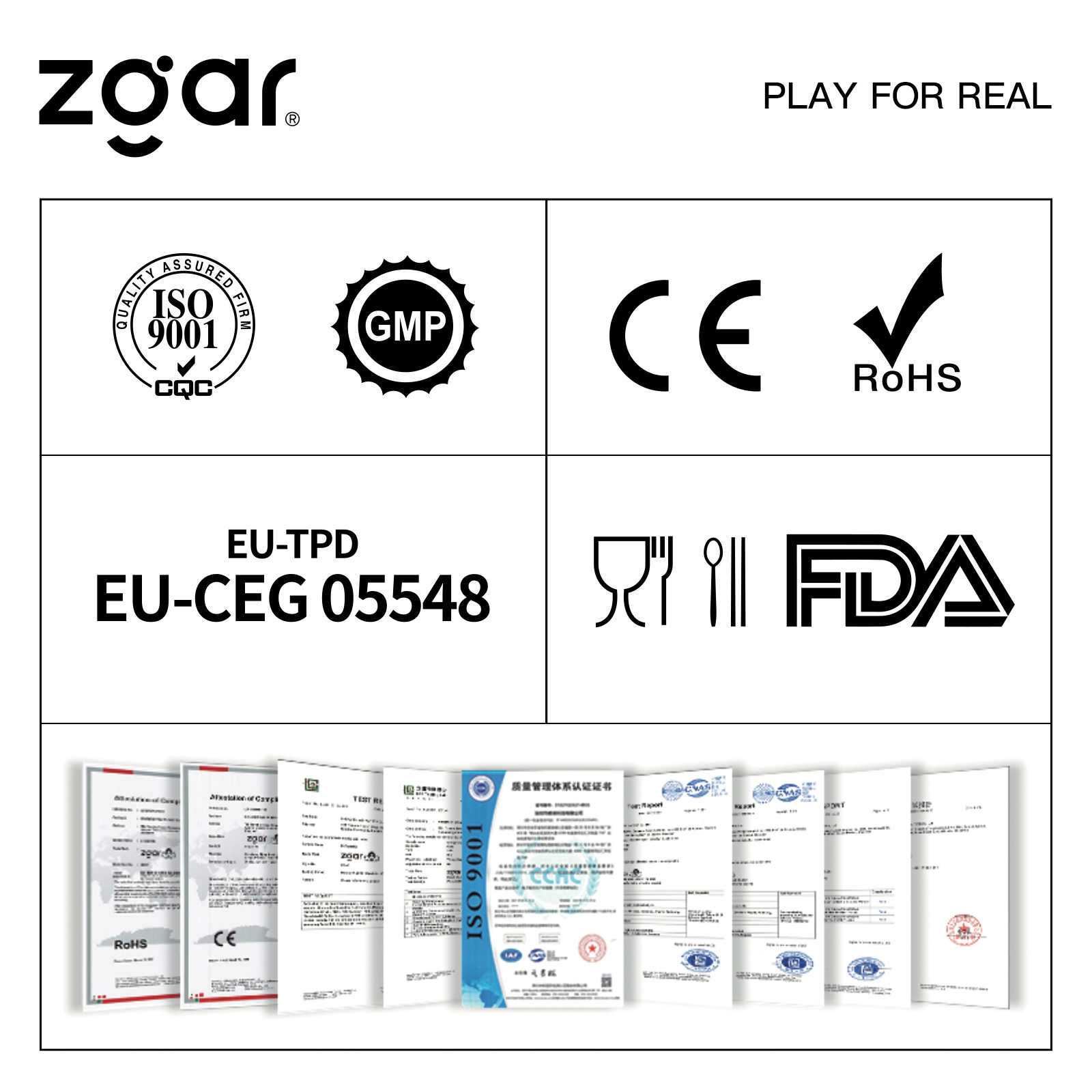
ZGAR electronic cigarette uses high-tech R&D, food grade disposable pods and high-quality raw material. A new design of gradient our disposable vape is impressive.We equip with breathing lights in the vape pen and pods.
Our team has very high requirements for product quality, taste allocation and packaging design. Designers only use Hong Kong designers, e-cigarette liquid only imports from the United States, materials are food grade, and assembly factory wants medical grade without ground workshop.
We offer best price, high quality Pod System Vape,Pods Systems Touch Screen,Empty Pod System, Pod Vape System,Disposable Pod device,Vape Pods to all over the world.
Pods,Vape Pods,Pod Systems,Atomizer, E-cigarette, Empty Pod Vape Manufacturer and Supplier in China
ZGAR INTERNATIONAL(HK)CO., LIMITED , https://www.sze-cigarette.com
