In the DRAM Storage Cell chapter, the structure of a single Cell is described. In this chapter, we will introduce how Cells are organized in DRAM.
In order to more clearly describe how the Cells are organized, we first abstract the DRAM Storage Cell in the previous chapter and finally get a new structure diagram, as follows:

DRAM is designed to make all of the Cells a Memory Array in a specific way. This section describes how DRAM organizes Cells in a specific form of Memory Array.
First of all, the simplest way to organize without considering the form is to hook up more Cells on a Bitline, as shown below:

However, in the actual manufacturing process, we do not limit the connection of Cells on Bitline. Because the more Cells that Bitline hooks, the longer Bitline will be, which means that Bitline's capacitance will be larger, which will cause Bitline's signal edge rate to drop (levels from high to low or from low to high). The rate) eventually leads to a drop in performance. To do this, we need to limit the total number of Cells attached to a Bitline and attach more Cells to other Bitlines.
From the structure diagram of Cell, we can see that in the structure of a Cell, there are two Bitlines, which are functionally equivalent, so we can spread the Cells to different Bitlines to reduce Bitline. length. Then, the way the Cells are organized becomes the following form:
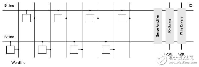
When both Bitlines are connected with enough Cells, if you need to continue to expand, you can only add Bitline. The added structure is as follows:
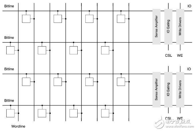
As you can see from the figure, after adding Bitline, the number of Sense Amplifier, Read Latch and Write Driver increases accordingly, which means that the cost, power consumption and chip size will increase. For this reason, in the actual design, priority will be given to increasing the number of Cells attached to Bitline and avoiding the increase in the number of Bitlines. This means that in general, the number of Wordlines will be much larger than that of Bitline.
In the figure above, a Memory Array consisting of 16 Cells is presented. The control signal has 8 Wordline, 2 CSL, 2 WE, and 1 Bit read and write operation at a time, which can be understood as an 8 x 2 x 1 Memory Array.
If you combine 2 CSLs and 2 WEs into 1 CSL and 1 WE, as shown in the following figure. At this point, this Memory Array has 8 Wordline, 1 CSL, 1 WE, and can read and write 2 Bits at a time, which is an 8 x 1 x 2 Memory Array.
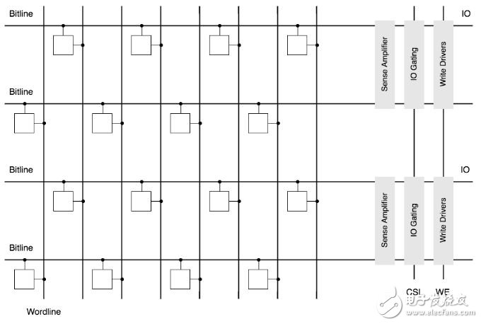
According to the above process, the number of Cells is continuously increased, and finally a Memory Array of mxnxw can be obtained, as shown in the following figure.
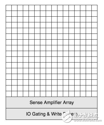
Where m is the number of Wordlines, n is the number of CSL and WE control signals, and w is a Bits that can be read and written.
In practical applications, we usually describe a Memory Array with Rows x Columns x Data Width. These definitions will be introduced in subsequent sections.
The Data Width of the Memory Array is the number of Bits accessed by the Array for a read or write operation. This number of bits is related to how the CSL and WE control lines are organized.
1.2 RowsThe Row in DRAM Memory has a one-to-one correspondence with Wordline. A Row is essentially all the Cells connected to the same Wordline, as shown in the following figure.
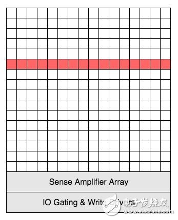
When DRAM reads and writes data, select a Row, which essentially controls the Wordline corresponding to the Row, opens the Cells, and caches the data on the Cells to Sense Amplifiers.
Row Size
The size of a Row is the number of Cells above a Row. One of the cells stores information about one bit, that is, the Row Size is the number of bits stored in a Row.
1.3 ColumnsColumn is the smallest unit that can be addressed in a Memory Array. There are n Columns in a Row, where n = Row Size / Data Width. The following figure is an example of a Column with a Row Size of 32 and a Data Width of 8.

Column Size
The size of a Column is the number of Cells contained on the Column, the same as the Data Width. Column Size and Data Width are essentially the same and are related to how the CSL and WE control lines are organized (refer to the description of CSL in the Memory Array section).
2. Memory BankPermanent magnet stepper motors use a permanent magnet (PM) in the rotor and operate on the attraction or repulsion between the rotor PM and the stator electromagnets.
MAINTEX's PM stepper motors are widely applied in many innovative applications, including: computer equipment, photographic systems, optoelectronic devices, valve control, ATM equipment, CNC machine, automatic winding machines, electronic clocks and medical equipment, etc.
Permanent magnet stepper motor,Pm stepper motor,Permanent magnet type stepper motor
Shenzhen Maintex Intelligent Control Co., Ltd. , https://www.maintexmotor.com
