The VB409 is a recently introduced power processing product. Its PENTAWATTHV (022Y) package is similar in size to the 7805 in the TO220 package, but has five pinouts. Another PowerSO10 package is a 10-pin surface mount IC. The input can be directly connected to the AC 220 V and the maximum input voltage allowed at the input is AC 580 V. There are two output sections: one is the final output OUTPUT1, which is +5V; the other is the chip's intermediate output OUTPUT2, which is typically 16 V. The power supply capability for the load is: OUTPUT1 is up to 80 mA and OUTPUT2 is up to 25 mA.

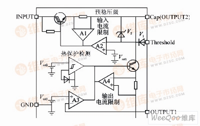
VB409 internal structure circuit diagram
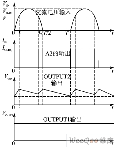
VB409 adopts the conduction angle technology, which automatically adjusts the on-time of each cycle according to the current of the load during one cycle of the alternating current. That is to say, power is absorbed from the power supply only in the low voltage portion of each positive cycle, thus greatly reducing power consumption, and the current output capability is three times that of the linear power supply. Its working waveform is shown in the figure.

Working waveform of VB409
As can be seen from the circuit diagram, the VB409 also has input and output current limits and thermal protection. Its function is to limit the output of the current when the output is shorted; on the other hand, the chip is turned off when overloaded.
It should be noted that the output range of OUTPUT1 is 4.75~5.25 V, the typical value is 5 V, the load current is increased by 1 mA, the output is 0.5mV, the accuracy is relatively high, and the output range of OUTPUT2 is 8~. 16V. Therefore, the output of OUTPUT2 is more suitable for use as a driving power source such as a relay. If you want to work as an amplifier, you need to perform another buck regulator.
Smart Watches
Smart Watches
everyone enjoys luck , https://www.eeluck.com
