The filter is a device used to eliminate interference noise, which can be used to effectively filter out the frequency point of a specific frequency or the frequency outside the frequency point. It occupies a very important position in the electronic field, and has been widely used in signal processing, anti-interference processing, power systems, and anti-aliasing processing. As for the programmable filter, the biggest feature of the system is that its filtering mode can be selected by program control, and the -3 dB cutoff frequency is programmable by program control, which is equivalent to a multi-functional filter and will have better application prospects. In addition, the system has the function of amplitude-frequency characteristic testing, and the oscilloscope displays the spectral characteristics, which can intuitively reflect the filtering effect.
1 Scheme demonstration and selection 1.1 Design and demonstration of variable gain amplifier moduleScheme 1: Digital potentiometer controls two-stage INA129 cascade. Use FPGA to control the digital potentiometer DS1267 to output different resistance values ​​as the feedback resistance of the high-precision instrumentation amplifier INA129. By controlling the digital potentiometer to change the magnification of INA129, the gain of the amplifier can be adjusted.
Option 2: Use variable gain amplifier AD603 to achieve. The variable gain amplifier is composed of R-2R ladder resistor network and fixed gain amplifier. The signal added at the input of the ladder network is attenuated and output by the fixed gain amplifier. The amount of attenuation is determined by the reference voltage added to the gain control interface. ; It can be controlled by a single-chip microcomputer, and a precise reference voltage is generated by the DAC to control the gain, so as to realize more precise numerical control.
Because the input sine small signal amplitude is 10 mV, the voltage gain is 60 dB, the 10 dB step control is adjustable, and the voltage gain error cannot be greater than 5%. In terms of accuracy, both schemes can be realized. Add one more level after AD603 Amplification can also achieve an amplification factor of 60 dB. However, the internal structure of the digital potentiometer is complicated and has the influence of capacitance, which will bring unexpected consequences after the subsequent stage is connected to the op amp, so scheme 2 is adopted.
1.2 Design and demonstration of filter moduleOption 1: Use digital filters. Use MATLAB's digital filter to design FIR or IIR filters. Digital filters have the advantages of high accuracy and good cut-off characteristics. However, the FIR filter will take up too much FPGA resources. The IIR filter is designed with heavy workload and low stability. In order to make the cut-off frequency adjustable, different parameters must be used, and the amount of software in the design is relatively large.
Option 2: Use a passive LC filter. Various types of filters can be built using inductors and capacitors. With reference to the relevant parameters in the filter design manual, an ideal filter can be designed relatively easily. However, if the cutoff frequency is to be adjusted, only the inductance and capacitance parameters need to be changed, and the hardware will be very complicated.
Option 3: Use an integrated switched capacitor filter chip. Switched capacitor filter is a large scale integrated circuit filter composed of MOS switch, MOS capacitor and MOS operational amplifier . Driven by the clock frequency, the switched capacitor group can be equivalent to an equivalent resistance related to the clock frequency. When the external clock is used to change, the equivalent resistance changes, thereby changing the time constant of the filter, and also changing the filtering characteristics. Switched capacitor filters can directly process analog signals without the need for A/D and D/A conversion like digital filters, which simplifies circuit design and improves system reliability.
In summary, this system adopts scheme 3, which uses integrated chip MAX297 to realize low-pass filter and LTC1068 to realize high-pass filter; adopts scheme 2, which uses passive LC filter technology to realize fourth-order elliptic low-pass filter.
2 System overall design scheme and realization block diagramThe system uses single-chip microcomputer and FPGA as the control core, and is composed of a controllable gain amplifier module, a program-controlled filter module, and an amplitude-frequency characteristic test module. The system block diagram is shown as in Fig. 1. The signal with input amplitude of 1 V is attenuated by the voltage divider network and becomes a small signal with amplitude of 10 mV, which is amplified by the OPA690 pre-stage 2 times, and plays the role of impedance transformation and isolation at the same time. At the same time, a sinusoidal signal with a set frequency is generated by AD9851, which is selected by the analog switch and sent to the subsequent stage. The signal is controlled by the program AD603 for 0~60dB adjustable gain amplification, and then sent to the filter module. The filter module includes low-pass, high-pass, and elliptic filters. The low-pass and high-pass are controlled by the program. The -3 dB cut-off frequency is adjustable from 1 to 30 kHz, and the step is 1kHz. The cut-off frequency of the elliptical filter is 50 kHz. Then through the simulation The switch selects a specific filter signal output, after the effective value detection and A/D conversion, it is sent to the FPGA to test the amplitude-frequency characteristics, and then two DAC0800s are used to realize the display of the amplitude-frequency characteristic curve.
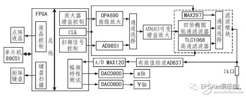
Figure 1 Overall block diagram of the system
3 Main functional circuit design 3.1 Amplifying moduleThe concrete circuit of the amplifying module is shown as in Fig. 2. The first part is a voltage divider network, in which the first 4 resistors attenuate the input signal by 100 times and form a 51Ω impedance with the internal resistance of the signal source, and the latter 51Ω is a matching resistor. The second part uses OPA690 to amplify the small signal by 2 times, while playing the role of impedance transformation and isolation. Since the input impedance of AD603 is 100Ω, a 100Ω resistor is connected in series at the back for matching. The third part is AD603 variable gain amplification, its gain increases linearly in dB as the control voltage increases. The reference voltage of pin 1 is obtained by calculating and controlling the output voltage of the DAC chip by the single-chip microcomputer, so as to realize precise numerical control. Gain G (dB)=40VG+G0, where VG is the differential input voltage, the range is -500~500mV; G0 is the starting point of gain, which is different when connected to different feedback networks. Connect a 5kΩ potentiometer to pins 5 and 7 to change.
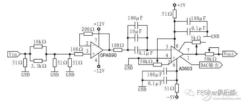
Figure 2 Enlargement module
3.2 High-pass filter moduleLTC1068 is a low-noise high-precision universal filter. When it is used for high-pass filtering, the cut-off frequency ranges from 1 Hz to 50 kHz, and there is no aliasing up to 200 times the cut-off frequency. Because the 4 channels of LTC1068 are low-noise, high-precision, high-performance second-order filters, each channel can realize the functions of low-pass, high-pass, band-pass and band-stop filters as long as a few external resistors are connected. The concrete circuit is shown as in Fig. 3. The Q value of port B is 0.57, and the Q value of port A is about 1. In the debugging of the circuit, it is found that the Q value of port A needs to be larger than the Q value of port B, otherwise the amplitude of the signal at the cut-off frequency will rise.
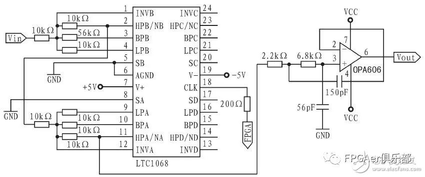
Figure 3 LTC1068 high-pass filter
The ratio of the clock frequency to the passband of the LTC1068 is 200:1. Since the LTC1068 internally doubles the clock signal CLK, when the cut-off frequency is at least 1 kHz, the internal clock frequency is actually 400kHz, so add another cut-off after the LTC1068 A low-pass filter with a frequency of 450kHz is used to filter out noise and high-order harmonics from the sub-band.
3.3 Low-pass filter moduleUse MAX297 to realize low-pass filter. The switched capacitor filter MAX297 can be set as an 8-order low-pass elliptic filter, the stopband attenuation is -80dB, and the ratio of the clock frequency to the passband frequency is 50:1. By changing the frequency of CLK, the filter can be -3 dB. The cut-off frequency is adjustable in the range of 1~20kHz, with a step of 1 kHz.
When using the MAX297, it should be noted that when the signal frequency and the sampling resolution are the same frequency, the switched capacitor group collects the same amplitude as the signal amplitude signal on the capacitor each time, which is equivalent to the case where the input signal is DC. The converter outputs a DC level. Similarly, when the signal frequency is an integer multiple of the sampling frequency, the same phenomenon will occur. For this reason, in front of it, an analog low-pass filter should be added to effectively eliminate high-frequency signals at the sampling frequency and above. Therefore, another MAX297 is used, and the cutoff frequency is set to 50kHz. The clock frequency is set to 2.5 MHz. After it, a low-pass filter is also added with a cutoff frequency of 150 kHz to filter out the high frequency components of the signal. The waveform is smoother. The concrete circuit is shown as in Fig. 4.

Figure 4 MAX297 low-pass filter
3.4 Fourth-order elliptical low-pass moduleThe system requires the production of a fourth-order elliptical low-pass filter with in-band fluctuation ≤1 dB, and a -3 dB passband of 50 kHz, which is realized by a passive LC elliptical low-pass filter. Use Fil te r Sol u ti on to simulate the simulation filter, and then simulate again in Mul TI sim and adjust the capacitance and inductance parameters to the nominal value. In addition, the relay stage follower before and after the elliptic filter avoids the shadow of the front and rear stages. The concrete circuit is shown as in Fig. 5.
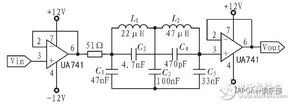
Figure 5 Elliptical low-pass module
4 System software designThe system software design consists of a single-chip microcomputer and FPGA. The user can select high-pass, low-pass and elliptic filters through the display of the interface, set the cut-off frequency, and display the amplitude-frequency curve at the same time. Among them, the single-chip microcomputer mainly completes the user's input and output processing and system control. The main functions of the FPGA are: control AD9851 to generate sweep signals, control the generation of clock signals for filter cutoff frequency, and control two D/A to display amplitude-frequency characteristic curves . The program flow chart is shown as in Fig. 6.
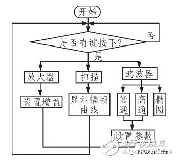
Figure 6 Program flow chart
5 Test plan and test results 5.1 Amplifier testThe frequency of the sinusoidal signal at the input of the amplifier is 10 kHz, the amplitude is 10 mV, and the gains are set to 10, 20, 30, 40, 50, and 60 dB respectively. Use an oscilloscope to measure the actual output amplitude and calculate the actual gain. The error is less than 1 %. In addition, the measured passband of the amplifier is 1~200kHz.
5.2 Low-pass, high-pass filter testSet the amplifier gain to 40dB and the filter to a low-pass filter. The preset filter cut-off frequency is in the range of 1~30 kHz, and the step is 1kHz. Use an oscilloscope to measure the actual cut-off frequency, and the calculated relative error is less than 1.5%, and 2fc The total voltage gain is less than 20dB. The high-pass filter test method is the same.
5.3 Ellipse filter testThe amplifier gain is set to 40 dB, and the actual -3 dB cut-off frequency and the total voltage gain at 200 kHz are measured with an oscilloscope. It is measured that fc=50.0kHz, and the amplitude is almost attenuated to 0 at 150 kHz.
5.4 Amplitude-frequency characteristic and phase-frequency characteristic testMeasure the frequency characteristics of low-pass and high-pass filters, and display the amplitude-frequency characteristic curve on the oscilloscope, which is consistent with the set filter mode and cutoff frequency.
6 ConclusionThe amplifier gain range of this system is 10~60 dB, the pass band is 1~200 kHz, the gain error is less than 1%. The filter cut-off frequency range is 1~30kHz, and the error is less than 1.5%. The elliptic filter cut-off frequency error is 0, at 150 kHz The amplitude is almost attenuated to 0. The error is mainly due to the clock frequency. When the cut-off frequency is 20 kHz, the highest clock frequency required is 2MHz, which cannot guarantee a good clock edge, and the clock frequency cannot be accurately controlled, and the amplifier The nonlinear error. In addition, the amplitude-frequency characteristic tester is realized by using DAC0800 and effective value detection circuit, and the overall performance of the system is good. Under the organic combination and collaborative control of the single-chip microcomputer and FPGA, the whole system works stably, with high measurement accuracy and flexible human-computer interaction.
Fitness Smartwatch
Fitness Smartwatch
everyone enjoys luck , https://www.eeluck.com
