Test and evaluation of the network performance of the antenna switch cabinet system
CAN bus is a serial data communication protocol developed by the German BOSCH company in the early 1980s to solve the data exchange between many control and test instruments in modern automobiles. Due to the high reliability and unique design of the CAN bus, it is currently widely used in power systems, mobile devices, medical and test instruments, and is recognized as one of the most promising field buses [1]. In November 1993, the International Organization for Standardization (ISO) officially issued the high-speed communication controller local area network (CAN) international standard ISO11898 [2], paving the way for the CAN bus standardization and standardization.
1 The feasibility analysis of the application of CAN bus in digital protection system
The CAN bus is a multi-master bus, that is, each node machine can become a master, and the node machines can also communicate. Each node on the bus shares the communication medium, so it is necessary to solve the conflict caused by the competition of the nodes to use the bus . The CAN bus uses a unique non-destructive carrier sense multiple access (NondestrucTIve CSMA / CD) bus arbitration technology based on message static priority [3].
The packet header identifier defines a static packet priority. As long as the bus is free, any node can start sending messages. If two or more nodes start transmitting messages at the same time, a bus access conflict will occur at this time. This conflict can be resolved by bitwise arbitration of the identifier. During arbitration, each transmitter compares the level of the transmitted bit with the level of the bus being listened to. If the level is the same, the node can continue to send; if it is different, quit sending.
The level on the CAN bus is represented by "dominant" (logic "0") and "recessive" (logic "1"). When both "dominant" and "recessive" appear at the same time, the result is the bus level Presented as "dominant". If node 1 sends a "recessive" level and node 2 sends a "dominant" level, the bus level heard by both nodes is "dominant", so node 1 loses arbitration and must Exit the sending state, and node 2 wins arbitration and can continue to send messages without being affected. The CAN bus, a non-destructive bus arbitration mechanism, ensures that messages and time are not lost.
In addition to the characteristics of the above non-destructive bus arbitration mechanism, the CAN bus also has the following remarkable features [4]: ​​①The CAN bus has a complete error handling mechanism, including listening, CRC check, bit filling technology, frame format check, etc. and Some corresponding guidelines. On the CAN bus, any node that detects an error will send out a series of bit streams called "error flags" to mark the damaged message. This message will be invalid and will automatically start to be retransmitted. Therefore, its reliability is very high.
â‘¡ The length of the data segment is at most 8 bytes, which will not occupy the bus time too long, thus ensuring the real-time nature of the communication. Such as
The serial rate of the MCP2510 CAN controller is 1M, and the longest message transmission delay is 64µs (8 × 8/1 = 64). But it also reflects the limitations of its inability to transmit long messages.
Considering the digital signals in the digital relay protection system, including the circuit breaker position status signal, protection input signal, opening and closing and alarm signal, etc., are all a few bytes of small data volume information, but they are real-time and reliable The requirements are very high. The application of CAN bus in the protection system to transmit digital signals can give full play to the technical advantages of CAN bus.
2 DSP McBSP and CAN controller interface design
The CAN bus communication module is composed of the CAN bus controller MCP2510 [5] of the MICROCHIP company and the CAN bus transceiver SN65HVD232 [6] of the TI company, as shown in FIG. 1. MCP2510 is a CAN controller with SPI interface, compatible with CAN2.0A / B protocol, supports passive / active version protocols of CAN1.2, CAN2.0A, CAN2.0B, and realizes logical link control and media access control of CAN bus , Can send and receive standard and extended messages, the bit rate can reach 1Mbps, it also has acceptance filtering and message management functions, including 3 transmit buffers and 2 receive buffers, reducing microcontroller (MCU) management The burden. SN65HVD232 is the drive interface between the CAN protocol controller and the physical bus. It provides different sending capabilities for the bus and different receiving capabilities for the CAN controller. It is compatible with the ISO11898 standard. 
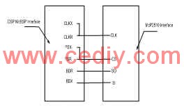
This article selects TI's high-performance C54 series DSP as the control core, the model is TMS320VC5410A, and the working frequency is 160MHz. TMS320VC5410A provides high-speed, bidirectional, multi-channel buffered serial interface McBSP and MCP2510 SPI (Industry Standard Serial Peripheral Interface) interface, the connection relationship between the two is shown in Figure 2.

McBSP has powerful functions and complicated structure. To achieve the communication between the two, the key is to properly configure each register of McBSP, including master-slave mode selection, clock signal, frame synchronization signal generation, edge selection of data transmission and reception, timing coordination, etc. Discussed separately below.
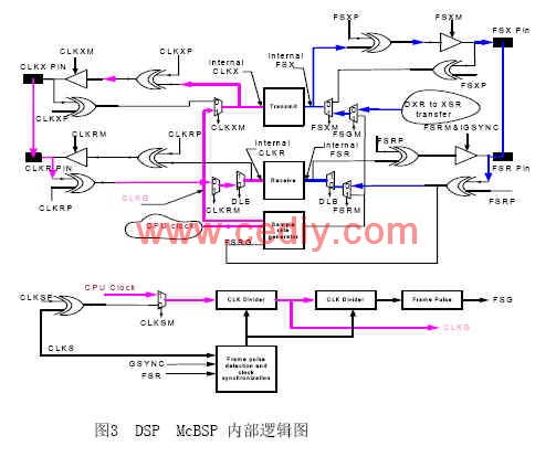
The connection relationship between the clock and the frame synchronization signal indicates that McBSP works in the master mode and the MCP2510 works in the slave mode. The sending clock of McBSP is generated by the DSP internal sampling rate generator (the sending clock mode bit CLKXM = 1), the sampling rate generator clock is generated by the DSP internal clock (the sampling rate generator clock mode bit CLKSM = 1), the receiving clock of McBSP is Send clock drive (receive clock mode bit CLKRM = 0), the clock of MCP2510 is given by McBSP. In short, all the clock sources are the internal clock of DSP; at the same time, send frame synchronization signal FSX from McBSP internal register DXR to XSR data copy The action is generated (transmit frame synchronization mode bit FSXM = 1, the sampling rate generator transmits frame synchronization mode bit FSGM = 0), and the received frame synchronization signal is driven by the transmitted frame synchronization signal (receive frame synchronization mode bit FSRM = 0).
According to the clock and synchronization signal flow analysis in the internal connection diagram shown in Figure 3, McBSP internal clock signals (Internal CLKX, Internal CLKR), frame synchronization signals (Internal FSX, Internal FSR) are synchronized with the MCP2510 clock signal and chip select signal Generate and stop. McBSP internal frame synchronization signal Internal FSX jumps from low level to high level, and the MCP2510 chip select signal connected to it is high level to low level effective, the phase is opposite, so the transmission frame synchronization of McBSP internal register The signal polarity bit FSXP = 1, and the McBSP internal frame synchronization signal Internal FSR and Internal FSX must be consistent, so the Internal FSR must also be inverted with the MCP2510 chip select signal, and the received frame synchronization signal polarity bit FSRP = 1. 
McBSP sends data on the rising edge of the internal clock CLKX, and receives data on the falling edge of the internal clock CLKR. Conversely, the MCP2510 receives data on the rising edge of the external clock CLK and transmits data on the falling edge of the external clock CLK. According to the previous analysis of the clock and frame synchronization signals: Internal CLKX, Internal CLKR and CLK are the same clock. To ensure reliable data transmission and reception, you must configure the transmit clock polarity bit CLKXP = 1 (Internal CLKX and CLKX are inverted) and receive Clock polarity bit CLKRP = 1 (Internal CLKR and CLKR are inverted). In this way, one side sends on the rising edge and the other side receives on the falling edge, and the communication is reliable; otherwise, both parties send and receive data on the same edge of the same clock, and reliable communication cannot be guaranteed.
3 Communication software process design
DSP transmits data through McBSP and SPI interface of MCP2510. The sending register of the MCP2510 serves as the mapping register of the sending buffer, and the DSP transfers the data to the sending buffer by accessing the sending register. The MCP2510 has 6 filters, and the data filtered by the receive filter on the CAN bus is first placed in the receive buffer. The receiving register serves as the mapping register of the receiving buffer, and the DSP accepts the data in the buffer by accessing the receiving register.

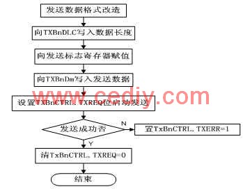
Figure 4 CAN send subroutine block diagram
The communication process between DSP and MCP2510 is divided into two steps: â‘ Configure the control register of McBSP according to the conclusions obtained from the above analysis, the sending process is: write the data into the sending register DXR of McBSP, and then send the data through the shift register XSR Moved out of pin BDX to send, the receiving process is: the data received through McBSP pin BDR is moved into the receive shift register RSR, and copy these data to the receive buffer register RBR, and then copied to the receive register DRR, and finally read in by the DSP. â‘¡ The communication between McBSP and MCP2510 exchanges data according to the clock and frame synchronization signals configured inside McBSP.
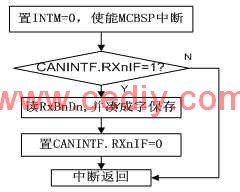
In order to improve the communication efficiency, DSP transmission adopts the active transmission mode, which is connected by the HD port of the DSP (configured as IO port) and the TXRTS terminal of the MCP2510 to select the transmission buffer unit. The transmission process is shown in FIG. 4; Once the MCP2510 receive buffer is full, it sends an interrupt signal to the DSP to inform the DSP to read the data. The receiving process is shown in Figure 5.

This paper analyzes the feasibility of the CAN bus in the digital protection system for the characteristics of good real-time and high reliability of the CAN bus short byte communication, and gives the hardware configuration scheme and software design of the interface between the DSP McBSP and the CAN controller Process. The data obtained from the actual communication test in the digital protection system proves that the CAN communication scheme is efficient and reliable, can meet the requirements of digital relay protection for real-time communication, and fully utilizes the advantages of the CAN bus.
The author of this article innovates: According to the characteristics of the CAN bus, the feasibility of the CAN bus application in digital relay protection is discussed, and the internal clock and synchronization signal flow of the high-speed, bidirectional, multi-channel buffered serial interface McBSP of the TMS320VC54X DSP is analyzed in detail. It is concluded that the master-slave mode selection of the interface between McBSP and the CAN controller, the generation of clock signals and frame synchronization signals, the edge selection of data transmission and reception, and the configuration of key bits of registers such as timing coordination.

Follow WeChat

Download Audiophile APP

Follow the audiophile class
related suggestion
