
This article is mainly about the relevant introduction of Samsung 788DF display, and focuses on the detailed distinction between Samsung 788DF display and 793MB.
Summary of common faults of Samsung 788DF displayA white LCD screen
A. A white screen indicates that the backlight board can work normally. First of all, determine whether the motherboard can work normally. You can press the power switch to check whether the indicator light responds. If the indicator light can change color, it indicates that the motherboard is working normally.
1. Check whether the connection line of the main board signal output to the screen has bad contact (the connection line or screen can be replaced).
2. Check whether the voltage of each operating point of the motherboard is normal, especially the power supply voltage of the screen
3. Use an oscilloscope to check line and field signals and clock signals (from input to output)
B. If the indicator light does not respond or does not light up, it indicates that the motherboard is not working properly
1. Check the voltage of each operating point of the motherboard, pay attention to the voltage of the EEPROM (about 4.8V), the reset voltage (high level or low level, depending on the model), and the MCU voltage. If there is a short circuit in the power supply, carefully find the location of the short circuit. There may be a short circuit in the copper foil of the PCB.
2. Check whether the MCU pins are in good contact with the motherboard:
3. Check whether the motherboard chip and MCU are working. Use an oscilloscope to measure whether the crystal oscillator starts to oscillate.
4. If necessary, replace the MCU or reprogram the MCU;
two. LCD black screen
A. First of all, determine whether it is the motherboard problem or the backlight board problem. You can check whether the indicator light responds. If the indicator light is not on, you should check the motherboard power section "
1. Use a multimeter to measure the working points of the main power supply, whether the fuse is blown, if it is blown, disconnect the power supply, use the resistance file to measure whether there is a short circuit at each main power supply working point, and carefully find the line if there is a short circuit (whether the copper foil of the circuit board is short-circuited ) And various related components (whether damaged or not connected with tin). } |3 S2
2. If there is no short-circuit phenomenon, you can refer to the white screen phenomenon for maintenance to ensure that the voltage and signal input and output of each operating point are in normal working conditions
B. If the working status of the motherboard is normal, check the backlight board
1. Check whether the connection between the main board and the backlight board is in contact with the main beam
2. Use a multimeter to measure the voltage of the backlight. There must be a power supply voltage of 12V, a switching voltage of 3.3V-5V and a backlight adjustment voltage of 0-5V. The switching voltage of the backlight is the most important. If there is no voltage or the voltage is too low, To check whether the output level of the MCU and the working state of the triode are normal, pay attention to whether there is a short circuit, and replace the components if necessary
three. Lack of color on LCD
1. Check whether there is a short-circuit or virtual solder between the main chip and the connector (pay attention to the chip feet, chip exclusion and connector, especially the flat socket)
2. Check whether there is bad contact between the screen and the motherboard connection line such as flat cable
3. If necessary, replace the motherboard, cable, and even the screen to find out the problem
four. The LCD monitor button does not work
1. Measure the voltage to the ground of each button. If the voltage is too low or 0, then check whether there is a short circuit, open circuit, pull-up resistance, false soldering, seat and connecting wire from the button board to the MCU. Poor contact
2. Pay attention to whether the button itself is damaged
Fives. The dual-color indicator of the LCD does not light up or only one color
1. Check the circuit of the indicator light. Whether the level of the triode controlled by the MCU output to the indicator light is normal, usually a high level 3.3V and a low level 0V. When the switch is switched on and off, the two levels will be reversed. If it is not normal, check whether there is a short circuit between the circuit and the MCU, or the solder joint
2. Check whether the power supply voltage (5V) of the triode is normal, whether the output of the triode is normal, and the voltage at both ends of the indicator light can be measured
3. Check whether there is poor contact between the motherboard socket and the key board, and whether the circuit board is short-circuited to the ground
4. It is necessary to replace the indicator
six. LCD color cast:
1. Check the main board signal R\G\B from the input to the main chip part of the circuit (whether there is a short-circuit with a virtual solder, and whether the capacitor resistance has an incorrect value)
2. Enter the factory mode, adjust the white balance, whether the normal color can be recalled
3. Replace the MCU or reprogram the MCU if necessary
Seven. LCD screen flower screen
1. Measure whether the main board clock output is normal
2. Check the main board signal R\G\B from the input to the main chip part of the circuit (whether there is a short-circuit with a virtual solder, and whether the capacitor resistance has an incorrect value)
3. Check whether there is a short circuit between the main board signal output and the connection socket output to the screen (IC pin exclusion and dual row pins, pay special attention to flat sockets)
4. Replace the screen if necessary
Eight. No signal on LCD:
A. No input signal appears after power-on (NO VGA INPUT)
1. Check the VGA cable connection
2. Check the main board from the line field input (note whether there is a short circuit between the line field of the VGA female socket and the ground) to the inverter output and then to the main chip part of the line (whether there is a virtual solder short circuit, whether the capacitor resistance has an incorrect value)!
3. Check the voltage of each operating point of the motherboard (it may be due to damage to the main chip)
B. Exceeding display (VGA NOT SUPPORT) or (FREQENCY OUT OF RANGE) appears after power-on
1. Check whether the computer input signal is out of range
2. Check the voltage of each working point of the motherboard (it may be due to damage to the main chip)
nine. The LCD screen flickers (word jitter)
1. Whether the "phase" can be adjusted with automatic adjustment or manual adjustment
2. Check the voltage of each working point of the motherboard (it may be due to damage to the main chip)
3. Check whether the capacitor resistance of the phase-locked loop has an incorrect value
4. Check the main board from the line field input to the inverter output and then to the main chip part of the circuit (whether there is a false solder short-circuit capacitor resistance and whether there is an incorrect value)
ten. LCD ghosting
1. Check the input signal, whether it is caused by the connection and distribution or the VGA cable is out of specification
2. Check whether the motherboard VGA socket is soldered or connected
3. Check the main board from the signal input to the chip part of the line for false soldering, short circuit, wrong value of capacitance and resistance
4. Check the voltage of each operating point of the motherboard (it may be due to damage to the main chip)
Samsung 788DF/793MB detailed comparative analysis1. Circuit principle analysis
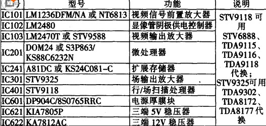
788DF/793MB color display is composed of power supply circuit, microprocessor circuit, line and field scanning circuit, RGB signal processing circuit, OSD screen display circuit, as shown in the figure below. As can be seen from the figure below, the machine mainly uses 10 integrated circuits and a small number of discrete components. The functions of the main chips are shown in the table below.
1. Power supply and energy saving control
(1) Power supply
The main power supply of this machine adopts IC60l (the actual products are mostly DP904C. The icon is 8S0765RRC, and the two are interchangeable. But it cannot be replaced with DP104, KA2S0880 and other ICs) as the core component of transformer coupling, separately excited switching power supply. As shown in the figure below, the functions of the DP904C pins are shown in the table below.
1) Power conversion
After the machine has input the mains voltage. The 220V voltage is sent to the line filter circuit composed of R601, R602, C601, L601, C602 ~ C604 through the fuse FHl. After filtering out the high-frequency interference in the mains power grid, it is sent all the way to the controlled degaussing circuit; the other is bridge rectified by the rectifier stack D601, and a DC voltage of about 300V is established at both ends of the C605. TH602 is a negative temperature coefficient thermistor, it can suppress the strong current of the impact generated by the initial charging of C605 at the moment of power-on.
The 300V voltage is sent to the IC601 pin (1) through the primary winding ((8)-(4) winding) of the switching transformer T60l to supply power to its internal switching tube. At the same time, the voltage is also passed through R610, R609 and the power switch SW601 (SW601). Not shown in the figure, connected to both ends of SW1 and SW2) to charge C606 and C607, and establish a starting voltage at both ends of them. When the voltage at both ends of C606 and C607 reaches 15V, the control circuit in IC601 starts to start, and the excitation voltage it generates makes the switch tube work in the on-off state.
The D603, R603, C608 and C609, R604, D604 externally connected to the IC601 (1) pin form a spike absorption circuit to prevent the switch tube from being damaged by the excessively high anti-peak pulse voltage at the moment when the switch is turned off.
After the switch tube works, the pulse voltage output on each winding of T601 is rectified and filtered to obtain a variety of DC voltages to supply power to the corresponding load. (1)-(2) The pulse voltage output by the winding is rectified by D606, R607 is current limited, C618 is filtered to obtain a DC voltage of about 33V, and then D607 is used to replace the starting circuit to provide IC601 with the working voltage after starting. The pulse voltage generated by (9)-(10) winding is rectified by D622 and filtered by C622 to obtain 7V voltage, which supplies power for Q623. The pulse voltage generated by the windings (10)-(11) is rectified by D625 and filtered by C629 to obtain a voltage of 50V. In addition to supplying power for the line output power, it also provides a detection voltage of 50V_SENSE for the microprocessor. The pulse voltage generated by the windings (12)-(13) is rectified by D626, filtered by C628 and C629 to obtain 80V voltage, which supplies power to circuits such as video output amplifiers. The pulse voltage generated by the (10)-(14) winding is rectified by D627 and filtered by C627 to obtain a voltage of 14.5V (14V in the figure), and this voltage is regulated by IC621 to obtain a voltage of 5V. It supplies power to circuits such as microprocessors and memory; the other way supplies power to Q625. The pulse voltage generated by the windings (15)-(16) is rectified by D628 and filtered by C631 to obtain a voltage of 14.5V (-14V in the figure), which supplies power to the field output circuit and the kinescope degaussing circuit.
2) Voltage stabilization control circuit
The main power supply voltage stabilization control circuit adopts PCC voltage stabilization method. When the mains voltage rises. After causing the on-current of the switch tube to increase per unit time, the energy stored in T60l reaches the set value in advance, so the pulse voltage generated by the sampling winding is rectified by D605 and filtered by C615. The voltage is formed by the voltage regulator tube ZD602, R610 The loop causes ZD602 to break down and turn on. When the voltage drop across R610 reaches 0.6V, Q601 turns on, the potential of IC601's (4) pin becomes low level, and the voltage comparator in IC601's (4) pin outputs in advance The high-level control signal makes the switching tube cut off in advance, shortening the on-time of the switching tube, and reducing the output voltage to a specified value to realize voltage stabilization control.
When the load becomes lighter, the discharge time of the filter capacitor is prolonged, so the voltage stored at both ends of C615 prolongs the conduction time of Q60l, the time for IC601 (4) pin potential to show low level is prolonged, and the conduction time of the switch tube is delayed. Because when the switch tube is cut off is determined by the horizontal frequency trigger pulse. Therefore, the on-time of the switch tube becomes shorter. Thereby avoiding the phenomenon that the output voltage of the switching power supply rises due to the light load.
When the mains voltage drops or the load becomes heavier, the control process is reversed. Another function of R610 is to make the discharge time of C615 close to the discharge time of the secondary filter capacitor of the switching power supply, shorten the response time of voltage regulation control, and improve the performance of voltage regulation control.
3) Protection circuit
The power protection circuit is composed of IC601 internal circuits and related components. Soft start protection:
During power-on time, the constant current source in IC601 charges the C611 externally connected to pin (4) through a 0.9A current. The voltage at both ends of it is gradually increased, causing the duty cycle of the excitation pulse output by the control circuit to gradually increase, so as to prevent the switch tube from being damaged by over-excitation when it is turned on.
Undervoltage protection: When the resistance value of the starting resistors R606 and R605 increases, or the power switch SW601 is in poor contact, C606 and C608 are leaking, and the Zener tube ZD601 is broken down. When the starting voltage provided by the starting circuit for IC60l is lower than 15V at the moment of starting, the control circuit in IC601 cannot be started; after starting. If the power supply system composed of D606, R607, C618, D607 is abnormal. Or the voltage stabilization control circuit and the load circuit are abnormal, and after the IC601 (3) rhyme power supply voltage drops to 9V, the under-voltage protection circuit makes the control circuit no excitation pulse output, and the switching power supply stops working, so as to avoid possible reasons such as insufficient excitation of the switching tube Cause damage.
Overvoltage protection; when the voltage regulator control circuit is abnormal. The control circuit in the lC60l cannot provide a controlled excitation pulse for the switch tube. Extend the on-time of the switch tube, causing the pulse voltage generated by each winding of T601 to increase. After the pulse voltage generated by the winding of T60l(1)-(2) is rectified and filtered, the voltage provided to the (3) pin of IC601 reaches 37V. , The overvoltage protection (OVP) circuit in IC60l operates to stop the switch tube and avoid overvoltage damage to the switch tube and load components.
In addition, if the voltage regulator control circuit abnormally raises the potential of IC601 (4) pin to 7.5V, the OLP circuit in IC601 outputs a protection signal, which will also stop the switching tube in IC601 to achieve overvoltage protection.
Over-current protection: When the load is short-circuited, the switch tube in IC601 is caused to over-current. After the voltage drop generated at both ends of the resistor connected to the s pole reaches 1V, the overcurrent protection (AOCP) circuit outputs a protection signal to stop the switch tube and realize the switch tube overcurrent protection.
Overheating protection: When the substrate temperature of IC601 reaches 160°C, the overheating protection circuit outputs a protection signal to stop the switch tube from working and avoid overheating and damage to the switch tube.
1. Work process
After the line-field oscillator and +B power supply control circuit in STV9118 work, the 28-pin of STV9118 outputs +B power supply PWM driving pulse, and after push-pull amplification by Q501 and Q502, the +B switch tube Q590 works in the on-off state.
During the on-time of Q590, the 50V voltage forms a loop through L501, Q590's D/S pole, R506 and ground. The current in the loop stores energy on L501; during the off period of Q590, the lower positive and upper negative induced voltages induced by L501, After being superimposed with a 50V DC voltage, D501 rectifies it to generate a power supply voltage of 10B proportional to the horizontal frequency at both ends of the filter capacitor C503. This voltage supplies power to the horizontal output tube Q490 through the primary winding of the dummy output transformer T501.
2. Voltage regulator control circuit
The voltage stabilization control circuit of the +B power supply is composed of the STV9118 internal +B control circuit as the core. The +B power supply has two control signals, one is the sawtooth signal input from the 16-pin of STV9118, and the sawtooth wave is sourced by the switch tube Q590 Resistor R506 is obtained by charging the 16-pin external capacitor C536 of STV9118; the other is the error signal input from 15-pin of STV9118. After the two are processed by the internal circuit of STV9118, they control the size of the 28-pin drive pulse duty cycle, and Q590 conduction time Perform control to achieve the purpose of stabilizing the +B voltage.
When the load becomes lighter and the +B voltage rises, the pulse voltage of each winding of the line output transformer T501 rises accordingly, so the line reverse pulse voltage generated by the 5-7 windings of T501 rises. The increased pulse voltage is rectified by D532, and the sampling voltage generated at both ends of C533 is increased, and then divided by R538 and R540, and R539 is current limiting, so that the voltage input from pin 15 of STV9118 is increased → the voltage of pin 14 is decreased → TDA9116 28 pin +B drive pulse high level time is shortened, that is, the switch tube conduction time is shortened → +B voltage drops. Otherwise, the control process is reversed.
Key reminder
If the resistance value of the 16-pin external resistor R508 increases, it will cause the charging time of C536 to be prolonged, resulting in the extension of the high-level time of the 28-pin output of the STV9118 (the on-time of the switch Q590) and the increase of the +B voltage, which will affect the secondary power supply. The switch tube, the line output tube and the picture tube all pose a threat. Because the machine is equipped with an X-ray protection circuit, at this time, the +B power supply and the line scan circuit will stop working.
In addition, it is not difficult to analyze that when the capacity of the 16-pin external capacitor C536 is reduced, the time constant of R508 and C536 will decrease, and the charging time will be shortened. The 28-pin output high level time will be shortened, and the control +B output voltage will drop.
If the resistance value of the resistor R506 increases, the voltage across R506 increases, that is, the charging voltage increases, the output high level time of pin 28 of STV9118 (the on-time of the switch Q590) is shortened, and the +B voltage drops.
When the 15-pin external resistor R539 is open, the voltage of 15-pin will drop very low, the voltage of 14-pin will rise, and +B will rise. At this time, due to the action of the X-ray protection circuit, the +B power supply and the line scan circuit will stop working.
3. Protection circuit
In order to ensure the normal operation of the line output power supply circuit and its load circuit, the power supply circuit is equipped with the following protection circuits.
(1) The spike absorption circuit + B power supply circuit is equipped with a spike absorption circuit composed of C502, R505, and D502 to prevent the peak voltage induced on the drain of the Q590 from being too high during the cut-off period of the Q590 and damaging the Q590.
(2) The soft-start protection circuit +B soft-start is mainly controlled by the voltage of pin 10 (HPOS) of STV9118, that is, the voltage of pin 10 HPOS during the soft-start period gradually increases as the external capacitor C437 is charged. , The voltage across C437 is 0, the soft-start circuit and protection circuit in lC will prohibit 26-pin HOUT (line excitation), 28-pin BOUT (+B drive) output, with the increase of the 10-pin voltage, first allow line excitation Output, the duty ratio of the line excitation pulse begins to increase; when the voltage of pin 10 continues to increase, pin 28 is allowed to have +B drive pulse output.
(3) Over-current protection circuit When the load over-current causes the S pole current of the switching tube Q590 to increase, and the voltage drop generated at both ends of R506 exceeds a certain value, compare it with the inverting input voltage of the C2 comparator in the 16-pin of STV9118 After that, the C2 comparator outputs a high level, the OR gate outputs a high level, the reset terminal R of the RS flip-flop is high, the Q terminal of the RS flip-flop resets and outputs a low level, and the NAND gate outputs a high level. The internal transistor T is turned on, the 28-pin of STV9118 outputs low level, and the +B switch Q590 is turned off, achieving the purpose of overcurrent protection.
(4) Overvoltage protection circuit line output transformer T501's 5-pin output line reverse pulse is rectified and filtered by D532, C533 to generate a DC voltage, after being divided by R536, R537, added to STV9118 pin 25 (XRAY), when 25 After the pin voltage exceeds the internal threshold voltage for a specified period of time, STV9118 enters the protection state and cuts off the line excitation output of pin 26 and the +B output of pin 28. To release the protection circuit, you need to cut off the power supply of STV9118 for a period of time, and then reconnect the display. The power supply is sufficient.
ConclusionThis is the end of the relevant introduction about the Samsung 788DF monitor. If there are any deficiencies, please correct me.
Related Reading Recommendations: Encyclopedia of Display High Voltage Bar Circuit Diagrams Related Reading Recommendations: How to deal with LCD flickerPvc Switch Box,Electrical Switch Box,Pvc Modular Switch Box,Electrical Pvc Switch Boxes
FOSHAN SHUNDE LANGLI HARDWARE ELECTRICAL CO.LTD , https://www.langliplastic.com