Semiconductor lighting industry is one of the subdivided industries of LED downstream applications. Under the wave of global low-carbon economy, the future of the semiconductor lighting industry is increasingly bright. Industry insiders expect the compound growth rate will exceed 30% in the next 5 years. China's competent authorities at all levels are also planning to issue corresponding support policies to promote the growth of China's semiconductor lighting industry.
It is reported that in the future, the obvious industry of China's semiconductor industry will enter the government's strong support, and companies will have their own supernatural powers. According to Guan Baiyu, deputy inspector of the Electronic Information Department of the Ministry of Industry and Information Technology, the Ministry of Finance is planning to promote semiconductor lighting related support policies; this year there are a number of national standards related to semiconductor lighting, the industry standards will be completed and submitted for approval procedures, while a number of standards Under research and development. In addition, considering the long industrial chain of semiconductor lighting, the product-related standards development process involves multiple departments. In order to do a good job in standard setting, the divisions will be joined together in the ministry to implement joint efforts among ministries and commissions, and will adopt production, learning, research, and joint working methods to fully promote the development of the semiconductor lighting industry.
Zhang Xiaofei, CEO of Gaogong LED, said that if the Chinese authorities follow the example of overseas developed countries and increase subsidies, China's semiconductor lighting industry will further accelerate. According to data from Japan, due to the subsidy policy implemented by the Japanese government, the share of semiconductor lighting lamps in Japan has rapidly increased from 0.01% in 2009 to 10% in February this year.
Local governments have begun to compete for the semiconductor lighting industry base, and accelerate the promotion and procurement of semiconductor lighting. Taking Dongguan as an example, since the Ministry of Science and Technology formally established as a pilot city for the demonstration project of semiconductor lighting application for “Ten City Millionâ€, Dongguan said that in 2011, a total of 40,000 lamps for semiconductor lighting were promoted. The project was a total of 2009-2011 In three batches of implementation, a total investment of 1.5 billion yuan was required. Chengdu also introduced relevant subsidy policies. From 2010 to 2012, Chengdu plans to implement LED lighting product application demonstration projects, promote the use of 400,000 LED lamps for lighting, and achieve investment of 645 million yuan in demonstration projects.
Many private equity funds have also begun to "bet" the semiconductor lighting industry. The chief partner of Saife Group believes that China's energy-saving lamps account for 70% of the world's total, but semiconductor lighting accounts for only 1% of the market. Taking into account the scale, technology, and quality of China's semiconductor lighting industry, the semiconductor lighting industry will have a competitive edge in the future.
According to the Orient Securities Research Report, according to the LED production process, the industry can be divided into upstream epitaxial wafer production, midstream chip manufacturing, and downstream chip packaging. Among them, upstream and midstream technologies have high technical content and high capital investment density. The most intense competition, the largest business risk areas. In the LED industry chain, LED epitaxial wafers and chips account for about 70% of the industry's profits, LED packaging accounts for about 10-20%, and LED applications also account for about 10-20%.
High Precision Multilayer PCB|multilayer printed circuit board
Product name:
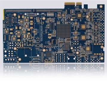
Industrial control board
Characteristic:
1, the board design
integration is very high;
2, the need to use composite
surface treatment method, gold finger plating hard gold 30 uinch;
3, gold finger position plate
thickness tolerance 1.6mm+/-0.10mm, it is recommended that customers in the
design of the gold finger corresponding to the inner line of the copper block,
in order to facilitate the plate thickness tolerance control.
Specifications:
Layer count: 6
Board thickness: 1.60mm
Base materials: FR4 S1141
Finished size: 172*148mm
Surface finish: Gold Plated +
finger
Line width/line space: 5/5mil
Minimum hole: 0.25mm
Solder resist color: blue
Cu thickness: inner layer 1 OZ
outer layer 1 OZ
Product name:
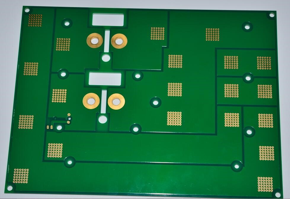
Thick Copper Board
Characteristic:
Prominent features: the outer
layer of copper thickness of 6 OZ, the inner product of copper thickness 6 OZ,
commonly used in large power equipment.
Processing difficulties:
1, inside and outside the need
to increase the thickness of copper thickness of 2 OZ or more by electroplating
method;
2, before pressing the need to
fill in the inner layer of resin;
3, the inner and outer layer
circuit is difficult to etch;
4, solder resist the need for
multiple printing.
 Specifications:
Layer count: 4
Board thickness: 3.0mm
Base materials: FR4 S1000-2
Finished size: 175*104mm
Surface finish:
Line width/line space:
12/12mil
Minimum hole: 0.5mm
Solder resist color: Sensitive
green
Cu thickness: inner layer 6 OZ outer layer 6 OZ
Product name:
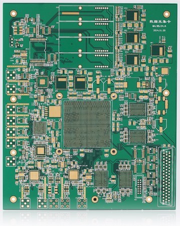
Data acquisition board
Characteristic:
1, the integration of the
board design is very high, thick diameter ratio of more than 10:1, heavy copper
plating is difficult;
2, the use of TG 170 plate
production.
Specifications:
1, the integration of the
board design is very high, thick diameter ratio of more than 10:1, heavy copper
plating is difficult;
2, the use of TG 170 plate
production.
Layer count: 8
Board thickness: 4.0mm
Base materials: FR4 S1000-2
Finished size: 400*400mm
Surface finish: mmersion
Line width/line space: 5/5mil
Minimum hole: 0.35mm
Solder resist color: Sensitive
green
Cu thickness: inner layer 1 OZ
outer layer 1 OZ
About Us:
BentePCB is a professional PCB manufacturing which is focus on double side, multilayer, HDI PCB , rigid PCB and Flexible PCB mass production. The company was established on 2011.
We have two factories together, The factory in Shenzhen is specialized in small and middle volume orders and the factory in Jiangxi is for big volumn.
Why Us?
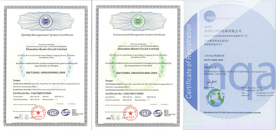
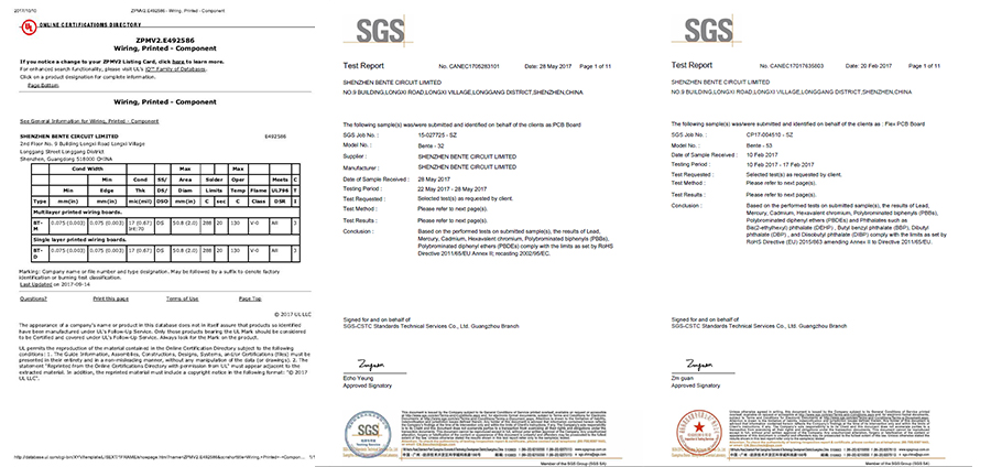
UL (E492586), ISO9001, ISO14001, TS16949, RoHS certified.
Turnover USD 10-50 million per year.
15,000 sqm area, 450 staff .
Mass Production from single to 16 layers.
Special Material:ROGERS, Arlon, Taconic.etc.
Client:Huawei, SAMSUNG, Malata, Midea,Texas Instruments.etc.
Certification(UL:E492586, TS16949, ISO14001, ISO9001,RoHS):
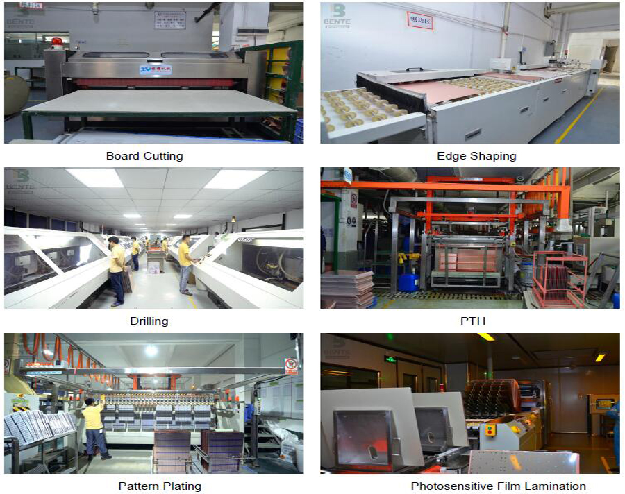
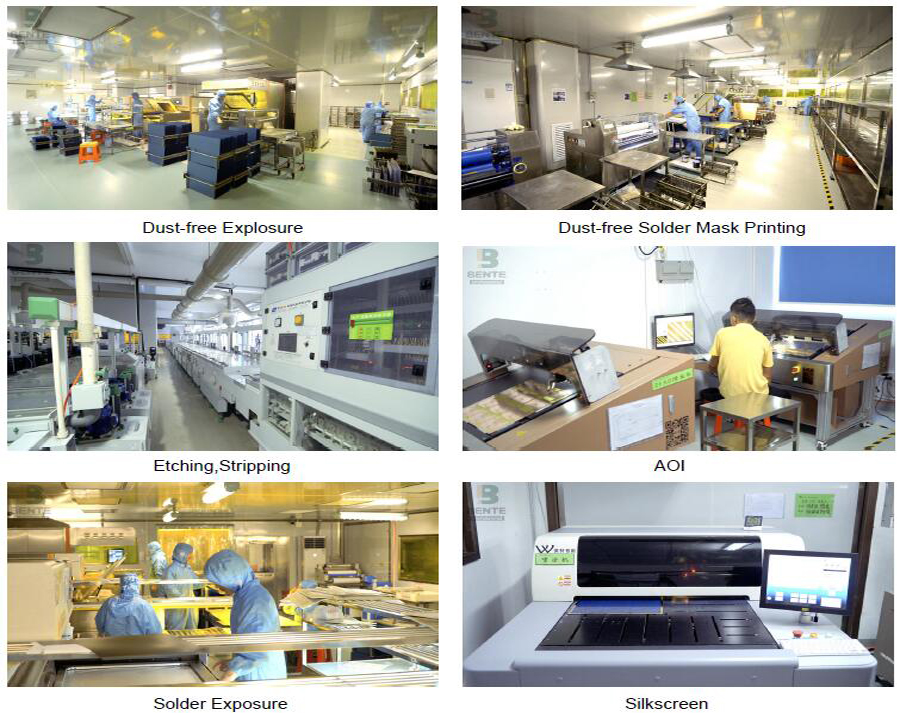
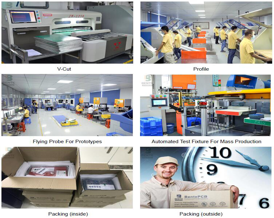
Factory Tour:
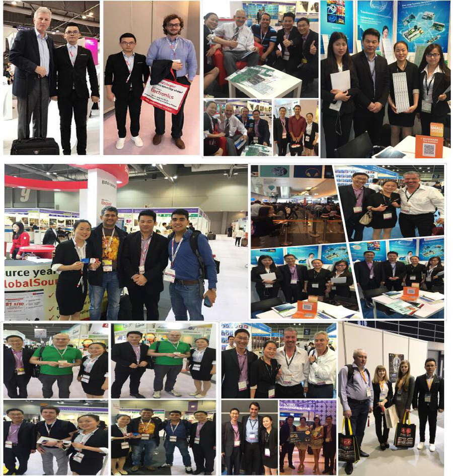
Exhibition:
We Took part in the famous exhibitions over the past years,and got highly appreciation from the top experts,as well as cooperated tightly with them.
Delivery:
BentePCB offers flexible shipping methods for our customers, you may choose from one of the methods below.


We don`t just sell PCBs .We sell sleep.

High Precision Multilayer PCB
High Precision Multilayer PCB, Multilayer Printed Circuit Board, Half Hole High-Precision Multilayer Board, High Precision Multilayer Board
Shenzhen Bente Circuit Limited , http://www.bentegroup.com
