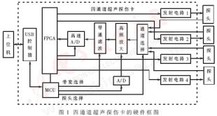
Four channels adopt time-sharing working mode. The four channels perform ultrasonic transmission in time-sharing, and the echo signal undergoes signal amplification and band-pass filtering after the channel selection switch, and then performs A / D conversion under the control of FPGA. In the dual-port RAM, the data is read by the microprocessor on the card, and after digital filtering again, it is transmitted to the upper PC through the USB interface.
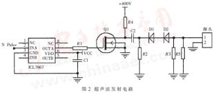
2 Ultrasonic transmitting circuit The four groups of transmitting circuits possessed by the four-channel ultrasonic flaw detection card are completely the same and adopt the time-sharing working mode. Normally, the four-way transmitting circuit is set to repeat working mode. The repetition frequency and the activation sequence of the probe are set by the user in the parameter setting items of the main interface of the microcomputer according to the specific conditions such as the thickness of the steel plate. Into the control system of ultrasonic flaw detection card. The activation of the transmitting circuit is completed by the FPGA. When the narrow pulse output by the FPGA is applied to a transmitting circuit, the transmitting circuit starts to work. The ultrasonic transmission circuit is mainly used to generate a high-voltage narrow pulse signal (400V). This high-voltage narrow pulse signal is loaded on the piezoelectric wafer of the ultrasonic probe, and converts electrical energy into acoustic energy (mechanical energy) to generate an ultrasonic signal. The ultrasonic signal transmission circuit of a single channel is shown in Figure 2. ICL7667 is a two-channel single-power FET driver that can convert weak TTL input signals to high voltage / strong current output with high conversion speed. The working principle of this circuit is: when there is no pulse to be emitted, the high-voltage power supply charges C2 through R4 and R2, so that the voltage difference between the two ends reaches + 400V. After the emission pulse arrives, the field effect transistor Q1 is turned on, and C2 is discharged through Q1. Because the voltage across the capacitor cannot be abrupt, the potential of the output of D2 is about -400V in an instant. This negative pulse acts on the ultrasound probe to cause piezoelectric transformation and emit ultrasound.
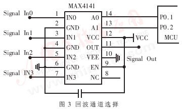
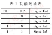
3 Echo channel selection Because only one (and only one) echo signal can be selected at the same time, the MAX4141 chip is used to complete the selection of the echo signal. The MAX4141 is a wideband (330MHz, 700V / μs), four-choice multiplexer chip with a buffer amplifier produced by MAXIM. It not only has a very fast switching rate, but also has high input and low output impedance Characteristics, so that the echo signal can be fully loaded on the programmable gain amplifier of the next stage. The echo signal strobe circuit is shown in Figure 3. Siganl In0 ~ Siganl In3 correspond to the echo signals of four probes respectively, and Signal Out is the echo signal after buffer driving and impedance conversion. The two signal lines given by the P0 port of the single-chip microcomputer are used for the channel selection of the MAX4141. The specific working conditions are shown in Table 1.
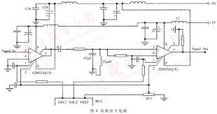
4 The echo signal of the high-frequency amplifier circuit is usually weak, so the high-frequency amplifier circuit is used to amplify the echo signal. Due to the different test objects (steel plate thickness), the strength of the echo signal is also uncertain, so when designing a high-frequency amplifier circuit, it is designed as a programmable amplifier circuit that can dynamically control the gain value, and its gain is dynamically controlled by the MCU control. In the design of the gain amplifier circuit, the AD603 variable gain, low noise operational amplifier was selected, which can achieve linear gain in the form of dB, with a gain value of 40dB per volt. The gain range can be selected in two ways through different connections to its pins, namely -11dB ~ + 31dB (bandwidth 90MHz) and 0dB ~ + 40dB (bandwidth 30MHz). In the design, two AD603 chips are used to form a programmable gain amplifier circuit through a two-stage cascade. The first stage is set to a gain range of -10dB to + 30dB, and the second stage is set to a gain range of 0dB to + 40dB. The AC coupling mode is used between the two stages to avoid the drift of the previous stage DC voltage to submerge the useful echo signal after being amplified by the latter stage. The gain control voltage (Gain Control Voltage) is controlled by the output of the D / A converter. The circuit connection in this design is shown in Figure 4. The gain range of the circuit is -10dB ~ + 70dB. For medium and thick steel plate flaw detection, it can fully meet the design requirements. The VREF in the figure is the output of the internal reference voltage of the D / A converter after being doubled. Its value is 2.4V. Since the voltage gain control terminal of the AD603 is very sensitive to small voltage changes, each stage in the design of the circuit Filter capacitors are added to overcome the effect of interference signals on voltage gain.
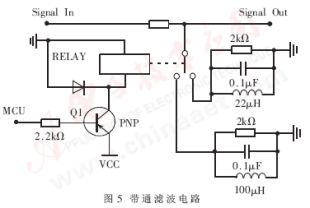
5 Band-pass filter circuit The band-pass filter circuit is used to filter the noise introduced during the amplification of the echo signal. Because the ultrasonic flaw detection card has four channels, the ultrasonic probes used in each channel are not necessarily the same, and different ultrasonic probes can be replaced in the same channel, so the filtering effect of using only one filter circuit will not be very good; and because the ultrasonic probe The transmission frequency range is wide, generally between 400kHz ~ 10MHz, so in this study, two sets of band-pass filter circuits are designed, and their bandwidth ranges are 400kHz ~ 2.5MHz and 2.5MHz ~ 10MHz, which can be driven by the microcontroller through the relay To strobe, the specific circuit is shown in Figure 5.
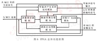
6 FPGA functional design FPGA is used as the core component of digital signal processing in this detection system. With its user-programmable characteristics and its high internal clock frequency, a data processing chip dedicated to ultrasonic detection is designed to make the entire detection system The detection speed is greatly improved. FPGA has a very important position in this system. Some data signal processing is done through it. Its internal functional block diagram is shown in Figure 6. As can be seen from the figure, the FPGA is mainly composed of a sampling delay module for narrow pulse generation, a parameter register module, a data acquisition compression module, a dual-port RAM module, and a defect automatic judgment module. For the specific working principle, see reference [3].
7 Microprocessor and USB interface The work of the entire board is controlled by the microprocessor (MCU). In this design, the host PC passes the control parameters to the MCU, including delay parameters, gain values, DAC curve, filter selection, etc., and then the MCU passes these parameters to the FPGA and gain controller (D / A conversion, respectively) Controller) to achieve board control. In addition, the MCU will digitally filter the data collected by the FPGA to improve the signal-to-noise ratio.
The data transmission between the MCU and the host PC is realized through the USB interface. The design uses the PILUSBD12 chip of PHILIPS, which is cost-effective, stable and reliable, and the ultrasonic echo signal is finally passed to the host PC for display and defect analysis. .
This paper introduces a hardware design method of four-channel ultrasonic flaw detection card for ultrasonic nondestructive testing, and develops an FPGA chip for echo signal processing and automatic defect judgment, which greatly improves the detection speed. The board can be used flexibly to construct various multi-channel ultrasonic flaw detection equipment.
references
1 Xilinx. The Programmable Logic Data Book. 1999, 2000
2 Carter. J W. Digital Designing with Programmable Logic Devices. NJ: PrenTIce Hall, 1997
3 Li X, Dong JW, Yu XY et al. Measuring System of the Level of Oilcan Based on Balance Principle. 2nd InternaTIonal Symposium on InstrumentaTIon Science and Technology, 2002.8, Jinan, China
The biggest difference between Home Theater Projector and ordinary business projectors is the resolution and ease of use. Most of the mainstream Home Theater Projectors have a resolution of 1080P Full HD, and are equipped with an intelligent system, which makes the projector more convenient to use. Home Theater Projector mainly pursues brightness, color, and contrast, which can bring users an immersive and realistic experience.
Features
1. Large screen: The size of traditional LCD TVs is mostly between 40-70 inches, while the Home Theater Projector can easily project 100-150 inches of screen content.2. Diverse uses: Home Theater Projector will be equipped with intelligent systems, which contain a large number of film sources. In addition, the projector can also be connected to different devices through different interfaces, such as game consoles, computers, U disks, etc. Only one machine can realize online drama, listening to songs, games, office and other functions.
3. Diffuse reflection eye protection: Home Theater Projector uses the principle of diffuse reflection to form images, which is less harmful to the eyes than the LCD screen.
4. Diverse usage scenarios: Home Theater Projector can adapt to different sizes of bedrooms, living rooms and even dedicated audio-visual room scenes due to its different brightness.
According to the increase of people's needs, the forms of Home Theater Projector are also becoming more and more diverse. In the past, people's impression of Home Theater Projector was mostly a square box placed on a cabinet or suspended from the ceiling, but there are already portable projectors that take into account both the sense of use and the size. In addition to portable micro-projectors, larger home laser TVs are also developing rapidly. Many users have abandoned traditional LCD TVs and opted for home projectors when decorating. It can also be seen from this that Home Theater Projector has a trend of gradually replacing LCD TVs.
home theater projector bluetooth,home theater projector setup,home theater projector hd,home theater projector 1080p,home theater projector led
Shenzhen Happybate Trading Co.,LTD , https://www.happybateprojector.com
