DS12887 is the latest clock chip of Dallas Semiconductor Corporation. It is made of CMOS technology. It integrates the crystal oscillator and external lithium battery related circuit of the clock chip into the chip. At the same time, it is compatible with the current clock chips MC146818B and DS1287 commonly used by IBM AT computers. Pin compatible, can be replaced directly. The clock circuit designed with the DS12887 chip does not require any peripheral circuits and has a good microcomputer interface. The DS12887 chip has the advantages of low power consumption, simple peripheral interface, high precision, stable and reliable operation, and can be widely used in various real-time clock situations requiring high precision. Its main functions are as follows:
(1) Contains a lithium battery, which does not lose data after running for more than ten years.
(2) Countdown, minute, hour, day, week, day, month, year, and have leap year compensation function.
(3) Binary digital or BCD code indicates time, calendar and fixed.
(4) 12-hour or 24-hour clock, 12-hour clock mode with PWM and AM guidance, with daylight saving time function.
(5) MOTOROLA5 and INATAEL bus timing selection.
(6) There are 128 RAM units and software speakers, 14 of which are used as byte clocks and control registers, and 114 bytes are general-purpose RAM. All ARAM cell data have power-down protection.
(7) Programmable square wave signal output.
(Interrupt signal output (IRQ) is compatible with the bus. The interrupt, periodic interrupt, and end of the clock update cycle can be blocked by software or separately.
Principle and pin description of DS12887
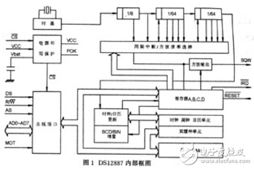
The internal principle of DS12887 is shown in Figure 1. It consists of oscillator circuit, frequency dividing circuit, periodic interrupt/square wave selection circuit, 14-byte clock and control unit, 114-byte user non-volatile RAM, decimal/binary adder, bus. Interface circuit, power switch write protection unit and internal lithium battery.

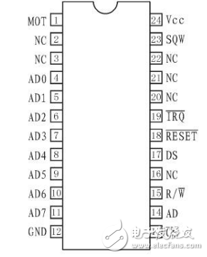
GND, VCC: DC power + 5V voltage. When the 5V voltage is within the normal range, the data can be read and written; when VCC is lower than 4.25V, the reading and writing is disabled, the timing function continues; when VCC drops below 3V, the RAM and timer are switched to the internal lithium battery.
MOT (mode selection): When the MOT pin is connected to VCC, the MOTOROLA timing is selected. When GND is connected, the INTEL timing is selected.
SQW (square wave signal is the same): The SQW pin can select one of the 13 taps of the internal 15-stage divider of the real-time clock as the output signal, and its output frequency can be changed by programming the register A.
AD0~AD7 (bidirectional address/data multiplexing line): Bus interface, which can interface with MOTOROLA microcomputer series and INTEL microcomputer series.
AS (address strobe input): Used to achieve signal separation, locking the address into the DS12887 on the falling edge of AD/ALE.
DS (data strobe or read input): The DS/RD guest has two modes of operation, depending on the level of the MOT pin. When using MOTOROLA timing, DS is a positive pulse that appears in the back of the bus cycle. Called data strobe; during the read cycle, the DS indicates that the DS12887 drives the bidirectional total time. During the write cycle, the DS's trailing edge causes the DS12887 to latch the write data. When INTEL timing is selected, DS is called (RD) and RD is the same as the definition of the allowable signal (OE) of a typical memory.
R/W (Read/Write Input): The R/W pin also has two modes of operation. When MOTOROLA timing is selected, R/W is a level signal indicating that the current period is a read or write cycle. When DSO is high, R/W high indicates the read cycle, and R/W low indicates the write cycle. INTEL timing, the R/W signal is a low level signal called WR. In this mode, the R/W pin has the same meaning as the write enable signal (WE) of the general-purpose RAM.
CS (chip select input): The chip select signal must be kept low during the bus cycle of accessing the DS12887.
IRQ (interrupt request input): Active low, micro interrupt input. The IRQ is in a high impedance state when no interrupt conditions are met. The IRQ line is an open-drain input that requires an external resistor.
RESET (Reset Output): When the pin is held low for more than 200ms, the DS12887 is effectively reset.
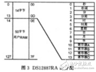
DS12887 internal function address allocation mapThe DS12887's underground distribution map is shown in Figure 3. It consists of 114 bytes of user RAM and 10 bytes of real-time clock time. Calendar and fixed RAM and 4-byte special registers for control and status, almost all 128 bytes can be read and written directly.

The time and calendar information is obtained by reading the corresponding memory bytes. The time, calendar and schedule are set or initialized by writing the corresponding memory bytes, and the byte contents can be in decimal or BCD form. The time can be selected from 12-hour or 24-hour system. When the 12-hour system is selected, the hour byte is set to logic "1" for PM. Time, calendar, and fixed bytes are double-buffered and always accessible. The 10 bytes per second take 1 second to check for a fixed condition. For example, when updating, the reading time and calendar may cause an error. There are two ways to use the three-byte fixed byte. The first type, when the fixed time is written into the corresponding hour, minute, and second decision unit, the scheduled interruption is started on time every day under the condition that the allowable trouble position is high. Second, insert one or more careless codes into the three fixed bytes. Don't care about the code is any hexadecimal number from C to FF. When the hour byte does not care about the code position, the time is set to occur once every hour because the phase line hour and minute fixed byte do not care about the bit, once every minute; when the three bytes are not care When interrupted once per second.
Nonvolatile RAMIn the DS12887, the 114-byte general-purpose nonvolatile RAM is not dedicated to any special functions, and they can be used as nonvolatile memory by processor programs. It is also accessible during the update cycle.
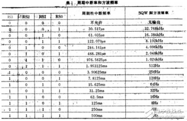
InterruptThe RTC real-time clock plus RAM provides three independent, automatic interrupt sources to the processor. The incidence of the interrupt is programmable, from once every second to once a day, and the rate of periodic interrupts can be selected from 500ms to 122μs. The update end interrupt is used to indicate to the program that an update cycle is complete. The interrupt control and status bits are in registers B and C, and the rest of this document will describe each interrupt occurrence condition in detail.
Crystal control bitWhen the DS12887 is shipped from the factory, its internal crystal is turned off to prevent the lithium battery from being consumed before the chip is loaded into the system. When BIT4~BIT6 of register A is 010, the crystal oscillator is turned on, the frequency division chain is reset, and other combinations of BIT4~BIT6 are used to turn off the crystal oscillator.
Square wave output selectionAs shown in the schematic of Figure 1, 13 of the 15 steps are available for the 15 to 1 selector. The purpose of the divider is to generate a square wave signal at the SQW pin. The frequency is determined by register A. RS0 to RS3 bit settings. The SQW frequency selection and the period interrupt generator are separated from the 15 select 1 selector. Once the frequency is selected, the switch of the SQW pin output is controlled by the program control square wave output enable bit SWQE.
Cycle interrupt selectionThe periodic interrupt can generate 500ms once every 122μs interrupt on the IRQ pin. The interrupt frequency is also determined by the register A. Its control bit is the PIE bit in the register B.
Update CycleThe DS12887 performs an update cycle every second and compares each certain byte with the corresponding time byte. If the matching three bytes are not concerned with the code, a random interrupt is generated.

ZGAR bar 600 Puffs
ZGAR electronic cigarette uses high-tech R&D, food grade disposable pod device and high-quality raw material. All package designs are Original IP. Our designer team is from Hong Kong. We have very high requirements for product quality, flavors taste and packaging design. The E-liquid is imported, materials are food grade, and assembly plant is medical-grade dust-free workshops.
Our products include disposable e-cigarettes, rechargeable e-cigarettes, rechargreable disposable vape pen, and various of flavors of cigarette cartridges. From 600puffs to 5000puffs, ZGAR bar Disposable offer high-tech R&D, E-cigarette improves battery capacity, We offer various of flavors and support customization. And printing designs can be customized. We have our own professional team and competitive quotations for any OEM or ODM works.
We supply OEM rechargeable disposable vape pen,OEM disposable electronic cigarette,ODM disposable vape pen,ODM disposable electronic cigarette,OEM/ODM vape pen e-cigarette,OEM/ODM atomizer device.

ZGAR bar 600 Puffs Disposable Vape, bar 600puffs,ZGAR bar 600 Puffs disposable,ZGAR bar 600 Puffs,ZGAR bar 600 Puffs OEM/ODM disposable vape pen atomizer Device E-cig
ZGAR INTERNATIONAL(HK)CO., LIMITED , https://www.szdisposable-vape.com
