Abstract: With the development of 3G networks, mobile phones will become the core hub of the information society. It is a demand to conduct remote monitoring and real-time monitoring at any time and any place. The mobile video surveillance system based on Micro2440 development board is introduced. The front-end video capture uses the ARM920t core embedded microprocessor S3C2440 as the hardware core and WinCE as the embedded real-time operating system. The transmission system adopts China Unicom's WCDMA wireless network, and the World Wide Web is used as the server. The back-end monitoring system driver development is completed in Platform Builder, and the application is completed in the EVC visual development environment. Through experiments, it proves that the system design is correct and reasonable: the pictures have been displayed in 3G mobile phones, the pictures are clear, the cost performance is high, and the system stability is good.
Keywords: WCDMA; mobile phone; ARM9; WinCE; video surveillance
With the rapid development of 3G network technology and the enhancement of various functions of 3G mobile phones, it has become possible to realize video surveillance anytime and anywhere by using 3G mobile phones. As embedded technology in today's IT industry, various embedded chips such as DSP, ARM, SOC, etc. are widely used in digital, security, traffic signal acquisition, telemedicine and other fields, and can predict future portable and multifunctional personal medical care. Digital service terminals will be as popular as mobile phones. Users can transmit their important physiological information to remote medical centers or home care experts in real time, accurately and quickly, so that they can get professional advice and guidance from doctors to realize telemedicine monitoring. Applications. The wireless monitoring system in the literature also uses ARM9 chip and WinCE operating system, but the software design part is not clear. The ARM-based wireless video monitoring system discussed in the literature only introduces the simple hardware structure and program flow chart. The experimental results, the literature only gives the simulation diagram, the 3G-based mobile phone remote monitoring system discussed in the literature only introduces the simple system block diagram and application examples, and there is no experimental result. The literature uses ARM9 core embedded chip and adopts Linux. The operating system, but there is no experimental verification, and the main discussion is the Linux kernel compilation. This paper designs a 3G mobile phone embedded video acquisition system based on ARM9 chip. Compared with the video acquisition system discussed in the reference, the system has the characteristics of small size, low energy consumption, convenient update and maintenance, and low development difficulty.
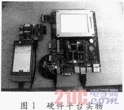
1 System hardware structure The hardware platform of the system is shown in Figure 1. In view of the reliability, scalability and maintainability of the system, the system adopts modular design principles. The video acquisition system hardware of the whole system consists of three parts.
This article refers to the address: http://
1.1 Microsystem Core Module This module consists of embedded microprocessor S3C2440A, NANDFALSH interface circuit, SDRAM interface circuit and bus interface circuit. The S3C2440 is a 32-bit RISC microprocessor chip based on the ARM920T core from Samsung. It provides a low-cost, low-power, high-performance small-scale microcontroller solution for handheld devices and general-purpose applications. The new bus architecture AMB-A is adopted, and its core also implements MMU, Harvard cache architecture. In addition, its enhanced ARM architecture MMU supports WinCE, Linux and EPOC32 operating systems, supports ARM modulation architecture, and supports booting from NAND FLAsH memory. Moreover, it also integrates a wealth of on-chip functions such as LCD controller, UART interface, USB master-slave interface, I2C interface, CAM IF unit and so on.
Although SDRAM cannot save data when it is powered down, it has a very high read/write speed, so it is suitable for the operation of the main program. The system uses two 32 MB models of HY57V561620 chip cascade to form 64 MB SDRAM memory. The internal memory structure of the chip is 4 Banks × 4M × 16 b, a total of 4 banks. The NAND FLASH storage system uses Samsung's K9F1208U0M chip with a storage capacity of 64M×8 b. The interface between the core module and the peripheral control module is implemented by the bus interface.
1.2 Video Acquisition Module This module uses the CMOS camera interface provided by the Micro2440 development board. It directly uses the CAM130 camera module provided by the friendly arm. The module consists of a 1.3 megapixel CMOS image sensor OV9650 and its interface circuit and power supply circuit. . The CMOS sensor is chosen because of its high integration, small size, low power consumption, easy programming, easy control, low cost, etc., and this type of sensor is developing in the direction of low noise and high sensitivity, so the CMOS sensor is currently The best choice for low pixel image acquisition systems. The interface circuit A/D converts and processes the image signal to the CAM IF of the processor. The microsystem core module controls the sensor through the I2C serial bus. The power supply circuit is supplied by the power conversion chip AS1117 to the camera with 1.8 V and 2.8 V voltages, of which 2.8 V is obtained by voltage division of the adjustable voltage chip (ie, VDD_CAM in Figure 2). The module's supply voltage is 3.3 V, which is consistent with the supply voltage of the microsystem core module and does not need to be separately provided.
1.3 Peripheral Control Module This module consists of LCD and touch screen interface circuit, JTAG debug interface circuit, USB master-slave circuit, reset circuit, power supply circuit, RS 232 serial port circuit and so on. The LCD and the touch screen interface circuit are used to display video data collected after the application is written, accept external control commands of the user, etc., and function as a human-machine interface. The JATG debug interface provides hardware debugging. It follows the IEEE 11491 standard and uses boundary scan technology to control the input and output signals of the chip through the boundary scan chain. An important function of JATG in this system is to burn the bootloader Bootloader into the development board for further kernel loading. The USB main port is used for devices that support the USB bus interface, such as an external USB flash drive, a removable hard disk, and a mouse, and can expand the storage space. The USB slave port is used to program the WinCE kernel file and communication between the system and the PC to the system. The reset circuit uses a special reset chip MAX811 with both power supply monitoring and data protection and a watchdog function to ensure reliable reset when the system is abnormal. RS 232 is used to view the startup of the Bootloader program and extend the serial communication function through HyperTerminal or DNW tools. The power supply circuit here provides 5 V (external power supply for the entire system), 3.3 V (core module, peripheral control, image acquisition module power supply) and 1.3 V (core module power supply).
2 Image sensor interface circuit and working principle The camera uses CAM130 module, the image sensor is OV9650, the schematic diagram and interface circuit of this part are shown in Figure 2.
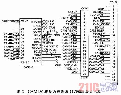
The interface between the OV9650 and the processor includes three parts: SCCB (Serial Camera Control Bus) interface, data output interface and control interface.
The SCCB interface functions to transfer the internal OV9650 internal register parameters provided by the processor. Its data line SIOD and clock line SIOC are equivalent to SDA and SCL in the I2C bus. That is to say, the SCCB functions as an I2C bus. The OV9650 is a slave to the I2C bus, and the S3C2440 is the corresponding master. The I2C bus uses serial mode to transfer byte data from high to low. After each byte is transmitted, the host controller sets SDA high and releases, waiting for the slave device to send an acknowledgment signal. The OV9650 has a 10-bit A/D converter embedded in it, corresponding to 10 data outputs D[0:9]. The format of the output image data can be 10-bit raw RAW, RGB or 8-bit RGB/YCbCr converted by internal DSP. The CAMIF unit of the microprocessor chip S3C2440 selected by this system supports 8-bit YUV/YCbCr format, so the data interface D[9:2] of OV9650 needs to be connected with the data port CAMDATA[7:0] of CAM IF. The XVCLK of the OV9650 is used to receive a 24 MHz operating clock from the CPU output. The three clock signals of the frame synchronization signal VSYNC, the line synchronization signal HREF, and the pixel clock signal PCLK generated by the OV9650 are transmitted to the ARM chip for controlling image acquisition. Each VSYNC pulse represents the beginning of one frame of image data acquisition, and the high level of HREF means that one line of image data is acquired, and the image sensor is in each PCLK from left to right.
One byte of data is sequentially acquired during the pulse process until all of the image data of one frame is acquired.
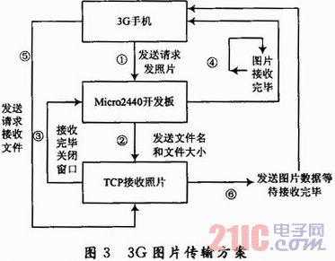
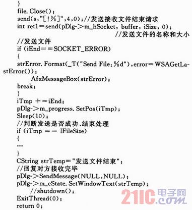
3 3G picture transmission process picture transmission flow chart shown in Figure 3, 3G mobile phone sends a text message request to the MINI2440 development board to send photos, ARM9 control center receives the information, send out the file name and file size, the TCP server receives the information received the picture And close the window, and at the same time, feed back the information that the picture has received to the 3G mobile phone, and then the 3G mobile phone sends a request to the server to receive the photo, and the TCP server sends the picture data to the 3G mobile phone until the picture is received, and when the receiving is completed, the 3G mobile phone feeds back the picture to the server. Received.
Some of the procedures for sending pictures on the Micro2440 development board and receiving pictures on the 3G mobile phone are as follows: 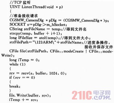
4 Application software design and experimental results The virtual serial port is used for communication between the operating system and the hardware platform. There are two limitations in EVC implementation of serial data communication: First, EVC does not support serial communication control MScomm, and the other is that WinCE does not support overlap I. /O operation. Therefore, the underlying development of data serial communication is to be carried out using WinCE API functions and multi-threading technology. The Windows API function treats the serial port as a file, and the operation of the serial port is similar to the operation of a normal file. In the EVC environment, open the serial port by calling the CreateFile function to set the serial port read and write mode: ![]()
Because WinCE does not support overlapping I/O, the sixth parameter of CreateFile cannot be set to: FILE_FLAG_OVER_LAPPED, which is set to the general constant "0", otherwise the serial communication processing will be blocked by the system information.
After opening the serial port, you can use the serial port initialization function SetCommState() to get the current configuration of the serial port, such as serial port number, baud rate, parity, data bit, stop bit, etc.: 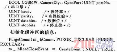
![]()
Application development is done in the EVC integrated development environment. Use EVC's AppWizard Wizard to create an MFC-based dialog program architecture. After performing the page layout "image display area", "initialization", "answer", "dial", "hang up" and other buttons, add various buttons for various buttons. The message response time and the setting of each button are completed in response to the command expected by the user. The "Initialize" button is used to initialize the 3G network. The “answer†button is a command that is sent to the development board in response to the 3G mobile phone. The “dial†button needs to be set with the number of the other party, the message sent when dialing, and the server IP and port number. After setting these, the dial-up wait response can be made. The "Hang Up" button enables the function of exiting the application and turning off the camera driver. It is relatively easy to add the click event response function of these buttons. In the EVC environment, double-click the button and enter the code editing area to program and debug. Here is a partial code for the "Initialize" and "Dial" buttons, followed by the omitted part. 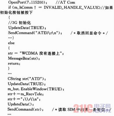
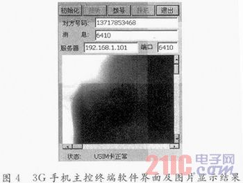
After the system application software development is completed, open the mobile phone host software in the 3G mobile phone application, click the “Initialize†button to complete the setting before “Dialingâ€, send the information to the Mi-cro2440 development board, wait for the response, and collect smoothly. The picture is finally displayed on the 3G mobile phone. Figure 4 shows the software interface and picture display result of the 3G mobile phone main control terminal.
5 Conclusion The system is based on ARM9 platform and WinCE operating system, collects live photo information through CMOS camera, and then connects to the web server through WCDMA wireless network. The mobile phone design software that meets the conditions, and finally realizes the function of picture monitoring on 3G mobile phone. . The system has the advantages of better real-time performance, lower cost and portability, and is very suitable for applications in security, transportation, handheld devices, home appliances, school patrol, etc. It is an important part of implementing video surveillance. At present, only the transmission of images and the display on the 3G mobile phone are realized, and the transmission of the video part is not completed due to time. The next step will be to use a suitable video compression coding algorithm such as H. 264, MPEG4 codec technology, to achieve video surveillance.
RFI Filter,Special Uses EMI Filter,Dc Inverter Filters,Low Pass EMI Filter
Jinan Filtemc Electronic Equipment Co., Ltd. , https://www.chinaemifilter.com
