Abstract: SoC is the development trend of VLSI and the mainstream of integrated circuits in the new century [1]. Its complexity, rapid design completion, cost reduction and other requirements determine that the design of system-level chips must adopt the method of IP (Intellectual Property) multiplexing. This article introduces the idea of ​​designing the IP core of the serial peripheral interface SPI (Serial Peripheral Interface) module with a reusable IP design method. It is implemented in Verilog language and verified by FPGA. It has passed the 0.25μm of TSMC (Taiwan Integrated Circuit Manufacturing Company). The process production line is streamlined to achieve the expected functions.
Keywords: SoC reusable IP SPI AMBA bus
introduction
?? With the rapid development of integrated circuit design technology and deep submicron manufacturing technology, the scale of integrated circuits has become larger and larger, and SoC (System on Chip, also known as system-on-chip) has appeared. Due to its advantages in speed, power consumption and cost, the development momentum is swift and violent. The SoC chip is a complex system. In order to complete the design within the specified time and improve the reliability of the design, the only way to rely on the SoC design method based on IP multiplexing. How to provide a reusable IP core for SoC design has become the basis and difficulty of SoC design.
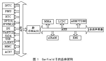
The ASIC System Engineering Technology Research Center of Southeast University has developed an embedded microprocessor code-named Garfield for the AMBA (Advanced Microcontroller Bus Architecutre) bus specification. In addition to the hard IP of the ARM7TDMI core of ARM Company, the microprocessor adopts the soft IP developed by itself for the other modules. This article takes the serial peripheral interface SPI as an example to introduce some experiences of IP design and verification based on multiplexing. This SPI module is based on AMBA's APB (Advanced Peripheral Bus, Advanced Peripheral Bus) specification, and can be used without modification in any microprocessor design that conforms to the AMBA bus specification.
The overall architecture of Garfield and the position of the SPI module in the system are shown in Figure 1.
1 SoC design method of reusable IP core
In system-level chip design, IP refers specifically to various proven super macro cell module circuits. According to the design level, VSIA (Virtual Device Interface Alliance) divides IP into three levels: hard IP, soft IP and solid IP in between. Hard IP has the best performance but poor adaptability, and soft IP has great flexibility and good portability. The IP core must have the following characteristics [2]: ①Readability; ②Design scalability and process adaptability; ③Testability; ④Port definition standardization; ⑤Copyright protection.
Code writing rules and synthesizable writing specifications are the basis for realizing IP cores, which can ensure the correctness of compilation and synthesis of IP soft cores under any EDA tool. In order to eliminate the risk of synthesis during SoC integration, we have formulated a Verilog code writing specification, and require detailed comments, which are easy for others to understand and modify. The reusable IP design process is shown in Figure 2 [3].
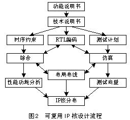
In order to easily integrate IP into the chip, a standardized interface or on-chip bus is required. VSIA has done a certain amount of work in this regard. In addition, it is necessary to separate the IP core interface part from the function part as much as possible in the design, and design it as a module alone. When it needs to be integrated into other interconnection protocols, only the interface part needs to be modified. To provide as much flexibility as possible, multiple parameters are allowed to be set during synthesis.
In the final user-oriented product release, the user manual is a very important part. This part of the document will be used for the selection, integration and verification of the IP core, and is a very specialized document. It mainly includes module system structure, functional block diagram, input/output port, timing diagram, calling method, design process, test guidance, recommended software compiler and driver, system verification guidance, debugging guidance and the IP core version history, etc. . In the release of reusable IP core products, multiple simulation models of the IP core should also be included for users to use in evaluation, design, and system testing. The simulation model of the IP core can generally be divided into three levels: â‘ behavior-level model, which can simulate all the functions of the IP core, including functions at the algorithm level and instruction set; â‘¡the hardware-level model, which can accurately provide the IP core Function and timing simulation; â‘¢Gate-level model, which provides a hard-core simulation model with timing back-annotation information.
In practice, we have explored a set of CVS (Collaborative Version Management System)-based version management and design and verification personnel to work together system procedures, made as comprehensive a simulation of RTL code as possible, provided a complete test vector, to ensure The quality of the final IP core has established standards and normative documents as required.
2 SPI module IP core design
Serial Peripheral Interface SPI (Serial Peripheral Interface) bus technology is a full-duplex, synchronous, serial data interface standard among a variety of microprocessors, microcontrollers and peripherals launched by Motorola [4]. The SPI bus is a three-wire bus. Because of its strong hardware functions, the SPI-related software is quite simple, allowing the CPU to have more time to process other transactions.
2.1 Interface signals and timing requirements of the SPI module
(1) The internal bus interface AMBA specification is an on-chip bus specification formulated by ARM. It provides the following advantages for SoC design: better portable and reusable design, low power consumption design, high performance and portable structure System design and better testability design [5]. SPI is the Slave module on the APB bus. APB bus timing is relatively simple, interested readers can refer to ARM's "AMBA SpecificaTIon" (Rev 2.0). Because this SPI module supports 3 types of DMA operations, in addition to the standard APB signal line, there are also 3 request signal lines connected to the DMA module.
(2) SPI bus interface and timing The SPI bus includes a serial synchronous clock signal line and two data lines.
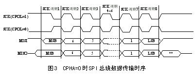
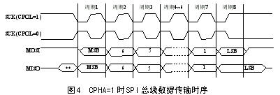
In order to exchange data with peripherals, the SPI module can configure its output serial synchronization clock polarity and phase according to the work requirements of the peripherals. The clock polarity (CPOL) has no significant impact on the transmission protocol. If CPOL=0, the idle state of the serial synchronous clock is low; if CPOL=1, the idle state of the serial synchronous clock is high. The clock phase (CPHA) can be configured to select one of two different transmission protocols for data transmission. If CPHA=0, the data is sampled on the first edge (rising or falling) of the serial synchronous clock; if CPHA=1, the data is sampled on the second edge (rising or falling) of the serial synchronous clock sampling. The phase and polarity of the clock between the SPI master module and the peripherals communicating with it should be consistent. The SPI interface timing is shown in Figure 3 and Figure 4 [4].
2.2 SPI module function design
According to the function definition and the working principle of SPI, the entire IP is divided into 8 sub-modules: APB interface module, clock divider module, sending data FIFO module, receiving data FIFO module, state machine module, sending data logic module, and receiving data logic module And interrupt formation module.
In-depth analysis of the four transmission protocols of SPI can be found, according to one protocol, as long as the serial synchronization clock is converted, the remaining three protocols can be obtained. In order to simplify the design regulations, if you want to continuously transmit multiple data, insert a serial clock idle wait between the two data transmissions, so that the state machine only needs two states (idle and working) to work normally. Compared with other designs, the idea is more refined and clear without basically degrading performance.
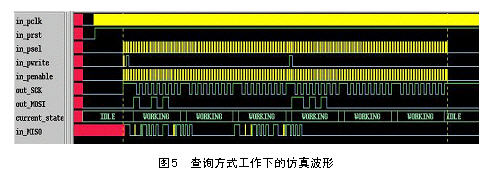
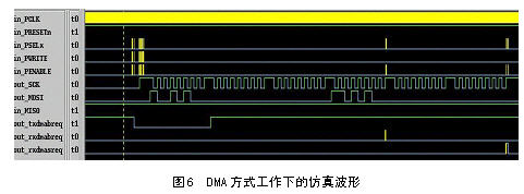
This SPI module has two working modes: query mode and DMA mode. The query mode learns its state by monitoring the status register of the SPI by the processor core, so as to determine the next action. In the DMA mode, the DMA module controls the exchange of data between the memory and the SPI without the participation of the processor core, which effectively improves the bus utilization.
3 EDA software simulation and FPGA verification
In order to ensure the robustness of the design, a variety of methods have been used to comprehensively simulate and verify the functions of this IP.
First, perform EDA software simulation verification. This kind of simulation includes RTL-level and gate-level simulation verification. RTL-level simulation just transfers the code file into the simulation software of the hardware description language for functional simulation to check whether the logic function is correct. Gate-level simulation includes pre-placement and post-placement simulation. After placement and routing simulation, you can obtain more accurate delay parameters, which can more truly reflect the behavior and performance of the module in actual work after the chip is manufactured. Therefore, through this type of simulation, the module design is considered successful and can be taped out. . To convert RTL-level codes into gate-level netlists, Synopsys’ integrated tool DC (Design Compiler) and Taiwan Integrated Circuit Manufacturing Company (TSMC)’s 0.25μm standard cell library are used.
To perform functional verification in the traditional design process, it is first necessary to add stimulus to the module that needs to be tested by writing test vectors, and then to judge whether the function of the module is correct by observing the output result of the module. But when writing the test vector, the test engineer does it on the basis of his own understanding of the module function. In this way, there is a problem. The excitation of the test vector to the module may be incomplete or wrong. Therefore, it is possible that the function of the module is wrong, but the excitation of the test vector does not reflect the error; it is also possible that the function of the module is correct, and the false positive error makes the verification process very inefficient [5]. In order to avoid the above problems, a system-level verification environment is adopted in the functional verification of the module. The environment is composed of IP bus, driver, monitor, external modules and scripts that coordinate their work. The modules that make up the system can be added to the environment as needed. Each verification process is a process in which the corresponding incentives act on the environment. The verification result is generated, tested and output by the environment. The verification environment is under the SOLARIS5.8 operating system, and the simulator uses Synopsys’ VCS, supports C/C++, Verilog and VHDL co-simulation, and can directly hang the SPI module in the verification environment and read it into the software through Verilog’s $readmemh task Incentives to be verified.
The simulation results of sending and receiving 6 bytes of data under the system clock of 66MHz, CPOL=1 and CPHA=0 are shown in Figures 5 and 6.
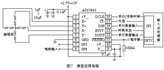
The typical application of the SPI module is to provide support for the touch screen by connecting with the touch screen control chip with SPI interface. For this goal, load the SPI module and other necessary modules into the FPGA for joint debugging of hardware and software, and verify the actual circuit. We chose the most common four-wire resistive touch screen, and the touch screen control chip uses ADS7843. ADS7843 is a serial interface chip with built-in 12-bit analog-to-digital conversion and low on-resistance analog switch. It supports 8 and 12-bit A/D conversion accuracy. In order to complete an electrode voltage switch and A/D conversion, the microprocessor needs to send a control word to the ADS7843 through the SPI interface first, and then read the voltage conversion value through the SPI interface after the conversion is completed. A standard conversion requires 24 clock cycles [6]. The typical application circuit is shown as in Fig. 7.
SPI's FPGA verification platform includes the Intergrator/LM-EP20K1000E and Intergrator/CM7TDMI development verification boards provided by ARM and the Garfield II verification circuit board (self-designed). Among them, the ARM7TDMI microprocessor core on Intergrator/CM7TDMI serves as the CPU of the entire development system. Through ARM MulTI-ICE, all modules including SPI necessary for verification are loaded into EP20K1000EFC672 of Altera APEX20KE series on Intergrator/LM-EP20K1000E board through JTAG port. The peripheral circuit is composed of Garfield II verification circuit board (including ADS7843) and touch screen. Through the software and hardware co-verification on the FPGA, and the SPI bus signal observed by the logic analyzer, it also proves that the SPI module has good performance.
In addition, through Taiwan Integrated Circuit Manufacturing Company (TSMC), using its 0.25μm standard cell library to conduct pipeline verification of the design many times, the actual IP circuit obtained is very stable in the prototype. So far, the design of IP is very successful. When designing SoC chips with similar architectures, they can be reused directly after configuring the corresponding parameters as needed.
Concluding remarks
Establishing a fully verified library of reusable IP modules with correct functions and good performance is the basis and requirement for rapid SoC design. To design a reusable IP, you need to follow certain design methods: complete and clear documentation; good code style; detailed comments; well-designed verification environment; test vectors with extremely high code coverage, etc. This article takes the SPI module IP as an example, in accordance with the standardized process and requirements, a preliminary attempt was made and good results were obtained.
references
1 Wei Shaojun. SoC design methodology. Electronic Products World, 2001(5): 36~38
2 Chen Lan, etc. SoC design technology. Computer Research and Development, 2002, l39(1):11
3 Shen Ge, et al. Research on SOC design methodology based on reusable IP. Journal of Xi'an Petroleum Institute (Natural Science Edition), 2003, l18:72
4 Xilinx Limited. CoolRunner-II Serial Peripheral Interface Master. 2002
5 Song Hongdong. Research on System Level Verification Method Based on Embedded Microprocessor and Implementation of Multimedia Acceleration Module [D]. [Master's Thesis]. Nanjing: Southeast University, 2003
6 Burr-Brown Limited. Touch Screen Controller ADS7843
7 David Flynn. AMBA: Enabling Reusable On-Chip Design. IEEE Micro. July/August 1997
Split Core Current Transformer
SCT 016 split core Current Transformer is widely used in measuring, electric power system, industrial control and other automation part. The hole diameter is 16mm. Input current can from 80 A to 120 A, and out put can be current and voltage. Current from 20mA to 1A, and voltage usually is 0.33V. Also we have terminal and wire lead out which is convenient and flexible. The accuracy class is 0.5%. we have exported to Europe countries, America and India. and got many good feedback from them.
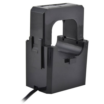
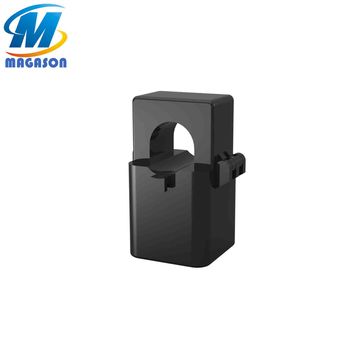
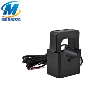
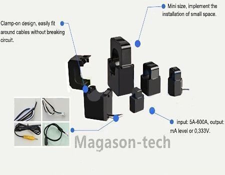
split core current transformer
- Lock type Crimping terminal output Suspension installation
- Measure current range: 5A~600A
- current Work voltage: 720V Flame resistance: UL94-V0
- Operation temperature: -25℃~+60℃
- Storage temperature: -30℃~+90℃
- Dielectric strength: AC 3500V/1min(between output and shell)
-
Isolation resistance: ˃100MΩ(500V DC) (between primary and secondary)
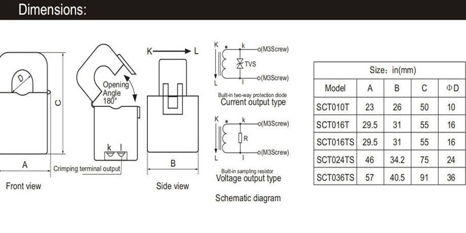
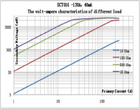
Core material: Nanocrystalline core 1K107 SCT016 Typical graph
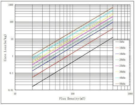
Core loss graph
-
Model
Rated measure current
Accuracy
Rated output
Work
frequency
SCT016 120A 0.5/1 40mA 50-1KHz
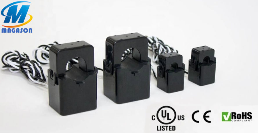 We attend Electrical exhibition In India, Germany and Brizil, South Korea...
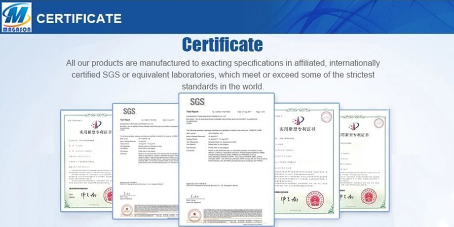
 All of our material meet the RoHs, UL , SGS, CE certification
FAQ
1-MOQ?
We will work hard to fit your MOQ .Small purchase quantity is ok.
2-Payment term?
T/T, Western Union, Paypal, Credit Card
3-Delivery port?
Shenzhen, Guangzhou, Zhongshan, Hongkong.
4-Shipping date?
About 7 days when we check the payment.
5-Do you produce the core and bobbin by yourself .
Yes.we have 2 head company,1 subsidiary company.one is bobbin factory,one is core factory,last one is transformer factory.
6-Where is your factory?
In ShaanxI
Split Core Current Transformer,Open Type Current Sensor,High Accuracy Current Transformer,Measuring Split Current Transformer
Shaanxi Magason-tech Electronics Co.,Ltd , https://www.magason-tech.com
