This article is mainly about the relevant introduction of Samsung 788DF display, and focuses on the detailed description of the relevant circuit of Samsung 788DF display.
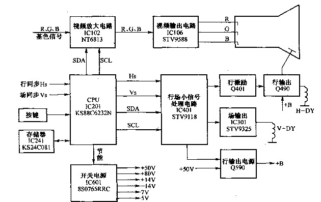
Analysis of internal structure circuit diagram of Samsung 788DF displayThe Samsung 788DF color monitor is compatible with VGA, SVGA, VESA, supports VESA flicker-free mode, the picture is stable and perfect, meets the "plug and play" function, provides intelligent power saving function, OSD screen adjustment function display, intuitive and convenient operation, and easy to use. The field scan chip STV9118 has a concise circuit structure. As shown in the figure, it is the circuit composition of Samsung 788DF.
It can be seen from the circuit diagram of the whole machine that the Samsung 788DF color display mainly uses line and field small signal processing integrated circuit IC401 (STV9118), line output, field output integrated circuit IC301 (STV9325), microprocessor IC201 (KS88C6232N), memory IC241 (KS24C081), video signal processing circuit IC102 (NT6813), video output circuit IC106 (STV9588) and switching power supply control circuit IC601 8S0765RRC (FS8S0765RRC) are the core components.

1. The working conditions of the microprocessor
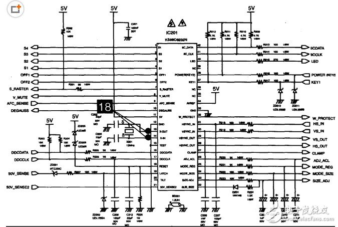
The microprocessor IC201 (KS88C6232N) must meet the following three conditions to work normally: one is a 5V supply voltage, the other is a reset signal, and the third is an oscillation signal.
1. Power supply circuit
The 5V voltage generated by the primary power circuit is filtered by C201 and directly applied to the 11 pin of the power supply terminal of the microprocessor IC201. Provides the voltage necessary for the microprocessor to work.
2. Clock oscillation circuit
All the work of the microprocessor is completed under the action of the clock pulse, such as storing/fetching data, analog quantity storage and so on. Only the function of the clock pulse makes the work of the microprocessor orderly. Otherwise, the microprocessor cannot work normally.
Microprocessor IC201 clock oscillator terminal 13, 14 feet internal circuit, crystal X201 and capacitors C202, C203 generate clock pulse signals. The clock signal is divided by the frequency divider to obtain the clock signal, which is used as the clock signal for the normal operation of the microprocessor circuit.
3. Reset circuit
The function of the reset circuit is to make the microprocessor start working from the initial state at the moment of power supply. The microprocessor IC201 contains a reset circuit, and the reset action of the CPU must be synchronized with the clock. After the reset is complete, IC201 enters the normal working state.
2. Synchronous signal processing circuit
The line and field synchronization signal sent by the host graphics card is sent to pins 31 and 30 of IC201. IC201 recognizes the current display mode according to the input line and field synchronization pulse, and outputs the line and field synchronization after switching polarity from pins 28 and 29 of IC201 The signal is sent to pins 1 and 2 of the line and field scanning chip IC401 (STV9118). At the same time, IC201 controls the whole machine through the bus, analog quantity and switch quantity control circuit.
Three, I2C bus control circuit
The IIC bus of IC201 has 4 pins: 16-pin (DDCDDATA), 17-pin (DDCCLK) are specifically used to exchange data with the computer host graphics card to achieve plug-and-play function; 42-pin (IICDATA), 41-pin (IICCLK) ) Used to control the line and field scanning chip IC401 (STV9118), the video amplifying processing circuit IC102 (NT6813) and the memory IC241 (KS24C081).
Four, offline detection circuit
The offline state is detected by IC201's 7-pin. When the color display is offline, IC201's 7-pin is in a floating state (voltage is 5V) because it is not connected to the host. After IC201 detects, it controls the color display to work normally status.
When the color display is connected to the host, pin 7 of IC201 is grounded through the host of the computer. If the host is not turned on at this time, the color display is in an energy-saving state. If the host is turned on at this time, the color display works normally.

1. Field scanning small signal processing circuit
The C331 externally connected to the 22-pin of the STV9118 is a field oscillation timing capacitor. After the STV9118 is in the working state, the C331 is charged and discharged, and a field sawtooth pulse is generated at both ends of the C331.
The vertical synchronization signal VS OUT output by the microprocessor circuit is added to pin 2 of STV9118 via R331, and after being processed by the internal synchronization signal input and polarity conversion circuit, it is added to the field oscillation circuit in STV9118 to make the frequency generated by the oscillator and The frequency of the vertical sync signal is synchronized. The field frequency of this machine has a large variation range. In order to achieve field synchronization under different field frequencies, it is automatically completed by the STV9118.
The field frequency sawtooth wave voltage formed by the field oscillator is divided into the following outputs: one way is sent to the geometric distortion control circuit, after being amplified by the amplifying circuit, and then respectively through the 32 feet (dynamic focus) and 24 feet (left and right pillow calibration) of STV9118 Output, provide field frequency parabolic pulse signal for dynamic focus circuit, left and right pincushion correction circuit and trapezoid correction circuit; the other way is amplified by the amplifier circuit and output the field sawtooth wave excitation signal from 23 feet.

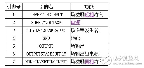
The 14V voltage output by the primary power supply circuit is rectified and filtered by D302 and C301 to provide a positive power supply for pin 2 of the field output circuit STV9325, and the -14V voltage output by the power supply circuit provides a negative power supply for pin 4 of the STV9325. D301, C306 and the on-chip circuit work together to complete the bootstrap boost function during the reverse stroke. During the field forward period, the 14V voltage is added to pin 6 of STV9325 via D301, and C306 is charged to the power supply voltage; during the field reverse stroke, pin 3 Output a field reverse pulse with an amplitude approximately equal to the power supply voltage, and add it to the negative terminal of C306, so that the reverse pulse voltage is superimposed with the original voltage on C306, so that the voltage at the positive terminal of C306 is approximately twice the power supply voltage. It is added to pin 6 of STV9325 as the working power supply of the field output stage during the field retrace period to shorten the field retrace time.
Pin 7 of STV9325 is the reference voltage input terminal of the internal amplifier. It comes from pin 13 of STV9118. The field sawtooth wave sent from pin 23 of STV9118 is added to pin 1 of STV9325 via R303. The amplified field sawtooth wave is output from pin 5. Go to the field deflection coil V-DY. R310 is a damping resistor to prevent V-DY parasitic oscillation. R308//R309 converts the field scanning current into voltage and adds it to pin 1 of STV9325 via R307 and C304 to form negative feedback to ensure the stability of the field output circuit amplifier operating point and avoid nonlinear distortion at the same time.
The field retrace pulse output from pin 3 of STV9325 is also added to the grid circuit of the kinescope for vertical blanking.
3. Field amplitude adjustment circuit
The field amplitude adjustment is carried out by changing the amplitude of the sawtooth wave signal output by the 23-pin of STV9118. When the field amplitude adjustment is performed, the microprocessor changes the amplitude of the field frequency sawtooth wave output by the 23-pin of STV9118 through the I2C bus, which is amplified by STV9325 After that, the amplitude of the current flowing through the V-DY can be changed to achieve the purpose of adjusting the amplitude of the field.
4. Field AGC circuit
When the color monitor works in different display modes, its field frequency changes. If no measures are taken, the field amplitude will also change when the field frequency changes. Therefore, some relevant measures must be taken on the circuit to compensate or stabilize the change of the field amplitude when the display mode of the color display changes. To keep the amplitude of the field excitation signal stable at different field frequencies, the circuit is realized by the AGC circuit in the field oscillation.
The 20 pin of STV9118 is the field amplitude control external capacitor terminal, and the 20 pin external field oscillation AGC external capacitor C332. When C332 is damaged, the field amplitude may change with the field frequency. Under the action of the field AGC, when the field frequency changes, the amplitude of the field oscillation (field excitation) signal can be kept stable, thereby keeping the field amplitude stable.
5. Field center adjustment and Moire elimination circuit
By adjusting the DC component of the 23-foot field frequency sawtooth wave of STV9118, the purpose of adjusting the field center can be achieved. In addition, the phase of the 23-foot field excitation signal of STV9118 is modulated by half-field frequency pulses to dynamically control the field center, which can also eliminate and improve vertical moiré fringes. Both the field center and the moir fringe are controlled by the microprocessor through the IIC bus.
ConclusionThis is the end of the relevant introduction about the Samsung 788DF monitor. If there are any deficiencies, please correct me.
Related reading recommendations: OLED display structure/features/principles Related reading recommendations: plasma display principles and structures, and analysis of advantages and disadvantagesFine Steel Cord For PU Timing Belts
Fine Steel Cord For PU Timing Belts
PU Timing Belts with steel cord, Timing belts truly endless or Jointed endless with cleats, for conveyor and Transmission Purpose
Our firm is providing an extensive series of PU Timing Belt with Steel Cord. Professionals use top quality material, which is sourced from truthful sellers of market to make this product. Our clientele can attain this product in varied specifications that meet on their necessities. Quality checkers also check this product on definite quality standards before delivery to the patrons.
Fine Steel Cord,Fine Steel Wire Rope,Pu Belt Steel Cord,Pu Timing Belt With Steel Cord
ROYAL RANGE INTERNATIONAL TRADING CO., LTD , https://www.royalrangelgs.com
