introduction
This article refers to the address: http://
The application of radio frequency identification (RFID) technology in logistics materials distribution, manufacturing, and postal services has become quite common. A tag antenna is a very important component of a radio frequency identification system that is responsible for receiving and transmitting signals that enter and exit the tag. The frequency bands allowed for RFID use in different countries are different, such as 920~925MHz (China), 952~954MHz (Japan), 868~870MHz (Europe) and 902~928MHz (USA). In order to enable the RFID system to operate in different bands at the same time, the antenna must have sufficient bandwidth or multi-frequency operation characteristics. To this end, techniques such as using thicker substrates, aperture resonance, coupled resonance, and load reactance can broaden the bandwidth of the antenna or enable the antenna to operate in both frequency bands simultaneously.
One of the design methods is to add a slot coupling structure to a dipole antenna operating at 910 MHz so that the antenna can also operate in the 2.45 GHz band. Based on this, this paper proposes a more compact dual-frequency RFID tag antenna. Compared to this antenna structure, the overall length is reduced by 10 mm, but good performance is also obtained. The dual frequency operation of the antenna can be achieved by selecting the appropriate coupling slot size. The dual-band antenna designed in this paper satisfies the -10dB return loss bandwidth of 840MHz to 940MHz (11%) and 2.26GHz to 2.56GHz (12%).
2 antenna design
The structure of the antenna designed in this paper is shown in Figure 1.

Figure 1 Dual-frequency tag antenna structure
The antenna was fabricated on an FR4 dielectric substrate having a relative dielectric constant of 4.4 and a thickness of 1.6 mm. The basic structure of the antenna is a symmetric dipole structure with a center feed. In order to make the antenna have dual-frequency characteristics, three coupling slits of length L2, L3, and L4 are added to the dipole structure of length L1. The current at the end of the dipole structure of length L1 and the current at the end of the coupling slit of length L2 are approximately 180°. Figure 2 shows the current distribution of the antenna surface. When the frequency is 910MHz, the current intensity distribution on the antenna surface gradually decreases from the center to the two ends. When the frequency is 2.45GHz, the current distribution on the antenna surface is mainly concentrated on the part of the antenna whose center length is about L2. This shows that the antenna can be seen as a combination of two independent dipole antennas, one of which is L1 in length, the working frequency band is near 910MHz, and the other length is L2. The operating frequency band is around 2.45 GHz. It can be seen that by controlling the lengths of L1 and L2, two different working frequency bands of the antenna can be adjusted.

(a) 910MHz (b) 2.45GHz
Figure 2 Surface current distribution diagram of the antenna
The simulation and optimization design of the above structure was carried out using Ansoft's electromagnetic simulation software HFSS. In the design, the initial values ​​of each parameter can be determined first based on literature and experience. The initial value can be determined according to the following method: For the lengths L1 and L2, according to the design theory of the symmetric dipole antenna, the selection criterion is an integer multiple of a quarter of the wavelength of the working band. The center frequency of the design is set to 910MHz and 2.45GHz, and the corresponding free-space wavelengths are 330mm and 122mm respectively. The length of L1 is twice that of a quarter wavelength, that is, 165mm; L2 is selected as a quarter wavelength, that is, 30mm. According to the results of the literature [6], other parameters are taken as L3=17mm, L4=24mm, W=15mm, W1=W2=5mm, S=d=1mm, Sfeed=2mm.
Based on the above parameters, simulation analysis was performed using HFSS. During the optimization process, it is found that as the length L2 increases, the higher resonant frequency of the antenna decreases toward the lower frequency band, while the lower resonant frequency hardly changes. Figure 3 shows the relationship between the change in length L2 and the resonant frequency of the antenna.

Figure 3 Antenna Return Loss vs. Length L2 Figure 4 illustrates how the slot width S affects the return loss of the antenna. When the slot width S is increased from 0.5 mm in steps of 0.5 mm to 3 mm, the higher resonant frequency of the antenna is gradually reduced from 2.58 GHz to 2.13 GHz, and the same lower resonant frequency is almost unchanged. The relationship between the return loss and the center width d is shown in Fig. 5. Obviously, when the width d changes, the return loss of the antenna remains almost unchanged.
Figure 4: Relationship between return loss and slot width S of antenna
Figure 5 Relationship between antenna return loss and width d
According to the above rules, by purposefully adjusting each parameter, the antenna can work in both ISO 18000-6 and ISO 18000-4 frequency bands and has good performance. Finally, after simulation analysis, the final design parameters of the antenna are: L1=134mm, L2=22mm, L3=17mm, L4=24mm, W=15mm, W1=W2=5mm,
S=d=1mm, Sfeed=2mm.
3 Results and analysis
Based on the simulation results, we made an antenna object, as shown in Figure 6.

Figure 6 Physical map of the dual-frequency tag antenna
The actual measurement results and simulation results of the antenna return loss are shown in Fig. 7. It can be seen from Fig. 7 that the actual measurement results are in good agreement with the simulation results. When VSWR<2, the designed antenna is in the bandwidth of ISO 18000-6 band, and the measurement result is 840MHz ~ 940MHz (11%), which is slightly smaller than the simulation result (840MHz~1.01GHz); and in ISO 18000-4 The bandwidth of the band is 2.26 GHz to 2.56 GHz (12%), which is not much different from the simulation result (2.31 GHz to 2.59 GHz). It can be seen that the antenna designed in this paper has a working bandwidth sufficient to cover both the frequency bands specified by ISO 18000-6 and ISO 18000-4.

Figure 7 Antenna Return Loss Measurement Results and Simulation Results The peak gain of the antenna is shown in Figure 8. From 900MHz to 920MHz, the gain is about 2.14–2.23 dBi; from 2.38GHz to 2.52GHz, the gain is about 5.30–5.70dBi. Figure 9 shows the simulation results of the antenna far-field radiation pattern. At 910 MHz and 2.45 GHz, the pattern of the H-plane is almost circular.

Figure 8 (a) Antenna peak gain (near 910MHz)

Figure 8 (b) Antenna peak gain (near 2.45GHz)

Figure 9 (a) Antenna radiation pattern (910MHz)

Figure 9 (b) Antenna radiation pattern (2.45GHz)
4 Conclusion
This paper proposes a dual-frequency slot-coupled RFID tag antenna and makes a physical object. The simulation results are in good agreement with the actual measurement results. The antenna is compact and has sufficient bandwidth for RFID tags that require both ISO 18000-6 and ISO 18000-4 bands. The disadvantage of this antenna is that although the antenna structure is relatively compact, the overall size of the antenna is still large. With the increasing use of RFID technology, RFID tags are also moving toward miniaturization and low cost. Therefore, the further work of this paper will be the miniaturization of tag antennas.
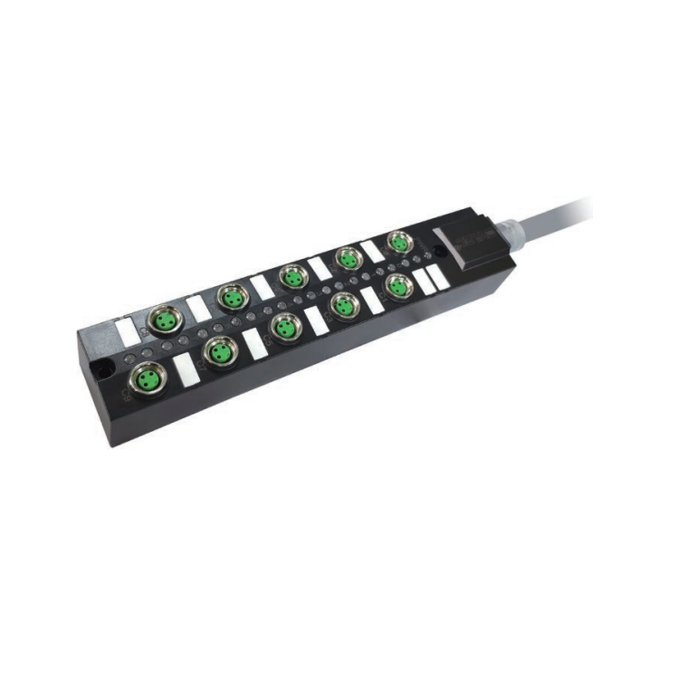
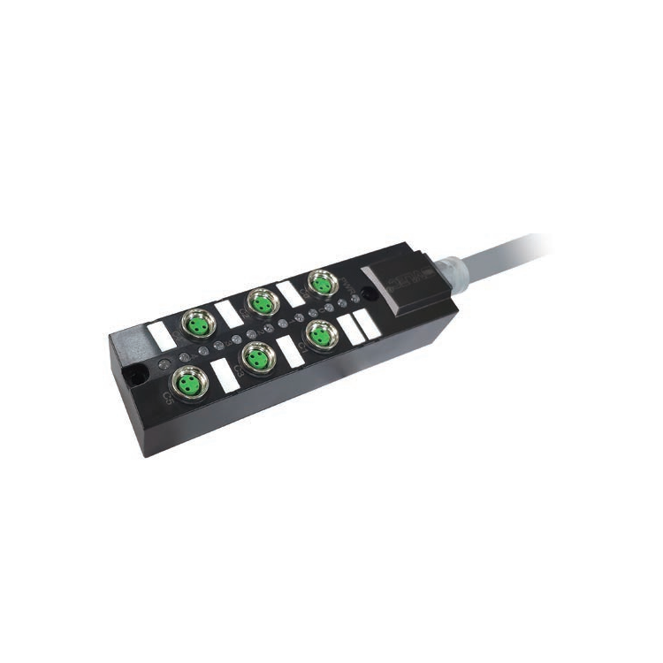
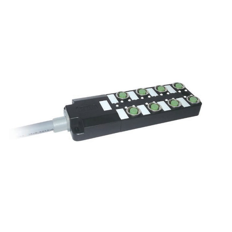
SVLEC provide M8 M12 junction box, which connects Sensors and actuators to the control system. They are ideal for harsh conditions, especially for cooling and lubricants. Fully encapsulated housing provides a higher level of protection and excellent shock and vibration resistance .


Distribution System,M8 Junction Box,M23 Input Distribution Box,Distribution Box with PCB plug,M12 Distribution System
Kunshan SVL Electric Co.,Ltd , https://www.svlelectric.com
